

How Does Resistive RAM Revolutionize Semiconductor Technology
OCT 9, 202510 MIN READ
Generate Your Research Report Instantly with AI Agent
PatSnap Eureka helps you evaluate technical feasibility & market potential.
ReRAM Technology Background and Objectives
Resistive Random Access Memory (ReRAM) represents a significant evolution in non-volatile memory technology, emerging as a promising alternative to traditional semiconductor memory solutions. The concept of resistive switching phenomena dates back to the 1960s, but intensive research and development efforts have accelerated dramatically over the past two decades as the limitations of conventional memory technologies became increasingly apparent.
The semiconductor industry has long followed Moore's Law, doubling transistor density approximately every two years. However, as traditional CMOS scaling approaches fundamental physical limits, alternative memory technologies have become essential for continued advancement. ReRAM technology leverages resistance changes in dielectric materials to store information, offering a fundamentally different approach from charge-based storage mechanisms used in DRAM and flash memory.
ReRAM's development trajectory has been characterized by significant breakthroughs in material science, particularly in understanding the formation and dissolution of conductive filaments within metal-oxide structures. Early research focused primarily on binary metal oxides like TiO2, HfO2, and Ta2O5, while recent advances have expanded to complex oxides and novel material combinations that enhance performance and reliability.
The primary technical objectives for ReRAM development center around achieving higher density, lower power consumption, faster switching speeds, and improved endurance compared to existing memory technologies. Current research aims to deliver ReRAM solutions that can operate at sub-10nm nodes with switching speeds below 10ns, endurance exceeding 10^12 cycles, and retention times of over 10 years at 85°C.
Beyond serving as a standalone memory solution, ReRAM technology aims to enable new computing paradigms. In-memory computing and neuromorphic applications represent particularly promising directions, as ReRAM's analog resistance states can naturally mimic synaptic behavior in neural networks. This capability positions ReRAM as a potential cornerstone for energy-efficient AI hardware accelerators and edge computing devices.
The technology evolution trend indicates a shift from traditional von Neumann computing architectures toward more specialized, memory-centric designs. ReRAM's ability to perform both storage and computational functions makes it uniquely suited for this transition, potentially revolutionizing how data-intensive applications are processed.
Industry objectives for ReRAM include not only replacing existing memory technologies in specific applications but also enabling entirely new device categories and computing approaches that were previously impractical due to the limitations of conventional semiconductor technologies. The ultimate goal is to overcome the memory wall that has increasingly constrained computing performance while simultaneously addressing growing demands for energy efficiency in an increasingly data-centric world.
Market Demand Analysis for Non-Volatile Memory
The non-volatile memory (NVM) market is experiencing unprecedented growth driven by the increasing demand for data storage solutions across multiple industries. Current market analysis indicates that the global NVM market is projected to reach $100 billion by 2026, with a compound annual growth rate exceeding 10%. This growth trajectory is primarily fueled by the expanding applications in consumer electronics, automotive systems, enterprise storage, and the burgeoning Internet of Things (IoT) ecosystem.
Within this landscape, Resistive RAM (ReRAM) technology is emerging as a disruptive force, addressing critical limitations of existing memory solutions. The demand for ReRAM is particularly strong in sectors requiring high-performance computing capabilities with minimal power consumption. Data centers, which currently consume approximately 2% of global electricity, represent a significant market opportunity for ReRAM technology, as operators seek more energy-efficient memory solutions to reduce operational costs and environmental impact.
The automotive industry presents another substantial growth vector for ReRAM technology. Advanced driver-assistance systems (ADAS) and autonomous vehicles require memory solutions capable of withstanding extreme temperatures and offering rapid data access with high reliability. Market research indicates that the automotive memory segment is growing at 15% annually, with ReRAM positioned to capture a significant portion of this expansion due to its inherent advantages in reliability and endurance.
Consumer electronics manufacturers are increasingly incorporating ReRAM into their product roadmaps, driven by consumer demand for devices with longer battery life and faster performance. The smartphone market alone, with annual shipments exceeding 1.3 billion units, represents a massive potential market for ReRAM integration, particularly as applications become more data-intensive and AI-driven.
Industrial IoT applications further amplify the market potential for ReRAM technology. The number of connected IoT devices is expected to surpass 25 billion by 2025, with industrial applications requiring memory solutions that combine longevity, reliability, and energy efficiency—all attributes where ReRAM demonstrates competitive advantages over traditional technologies.
The healthcare sector is emerging as another promising market for ReRAM adoption. Medical devices, particularly implantable and wearable technologies, benefit from ReRAM's low power consumption and radiation hardness. Market analysis suggests that the medical device memory segment will grow by 12% annually through 2027, creating additional opportunities for ReRAM deployment.
Despite these promising market indicators, challenges remain in achieving mass-market adoption. Price sensitivity continues to be a significant factor, with conventional memory solutions benefiting from economies of scale that ReRAM has yet to achieve. However, as production volumes increase and manufacturing processes mature, the cost differential is expected to narrow substantially, accelerating market penetration across multiple sectors.
ReRAM Development Status and Technical Barriers
Resistive RAM (ReRAM) technology has reached a significant level of maturity in recent years, with numerous research institutions and semiconductor companies demonstrating functional devices. Currently, ReRAM exists in various stages of development, from laboratory prototypes to early commercial products. Several companies including Weebit Nano, Crossbar, and Fujitsu have announced ReRAM products, while major semiconductor manufacturers like Samsung, Intel, and Micron have extensive ReRAM research programs.
The technology has demonstrated impressive characteristics including sub-10nm scalability, switching speeds in nanoseconds, and endurance cycles reaching 10^12 in laboratory conditions. Commercial ReRAM devices typically achieve endurance of 10^6 to 10^9 cycles, which is competitive with NAND flash but still below DRAM capabilities. Power consumption has been reduced to picojoule levels per switching operation, making ReRAM highly energy-efficient compared to conventional memory technologies.
Despite this progress, ReRAM faces several critical technical barriers that impede widespread adoption. The most significant challenge is the variability in resistance states, which affects reliability and yield. Cell-to-cell and cycle-to-cycle variations can lead to read errors and data corruption, particularly as device dimensions shrink. This variability stems from the stochastic nature of filament formation and rupture processes in oxide-based ReRAM.
Another major hurdle is the sneak path current problem in crossbar arrays, which limits the practical size of ReRAM arrays without selector devices. While various selector technologies have been proposed, including transistors, diodes, and threshold switches, each introduces additional complexity and potentially compromises the density advantage of ReRAM.
Material stability presents another challenge, as the repeated formation and dissolution of conductive filaments can lead to degradation of the switching layer over time. This affects both the endurance and retention characteristics of ReRAM cells. Researchers are exploring various material systems, including HfOx, TaOx, and TiOx, to optimize the trade-off between switching performance and long-term reliability.
The integration of ReRAM with conventional CMOS processes also poses significant challenges. While ReRAM is generally considered CMOS-compatible, issues such as thermal budget constraints, contamination concerns, and process variations must be addressed for high-volume manufacturing. Back-end-of-line (BEOL) integration is particularly challenging due to temperature limitations and potential damage to existing interconnect layers.
Scaling ReRAM to advanced technology nodes below 10nm introduces additional complexities related to quantum effects, variability, and reliability. As dimensions shrink, the statistical nature of filament formation becomes more pronounced, potentially limiting the practical scaling of ReRAM technology without fundamental innovations in materials and device architecture.
Current ReRAM Implementation Approaches
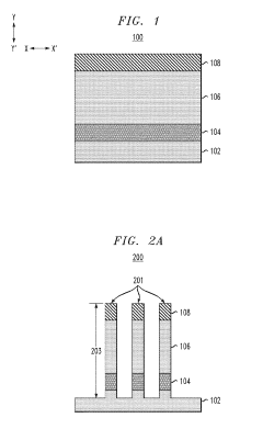
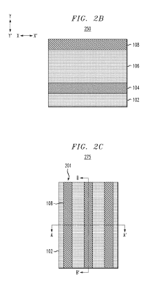
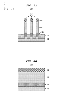
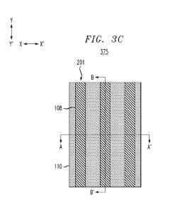
01 RRAM device structures and fabrication methods
Resistive Random Access Memory (RRAM) devices feature innovative structures that enable revolutionary memory performance. These structures include specific electrode configurations, resistive switching materials, and novel fabrication techniques that enhance reliability and performance. The manufacturing processes involve precise deposition methods, patterning techniques, and integration approaches that allow for high-density memory arrays with improved switching characteristics.- RRAM device structures and fabrication methods: Resistive Random Access Memory (RRAM) devices feature innovative structures that enable resistance-based data storage. These structures typically include a resistive switching layer sandwiched between electrodes. Advanced fabrication techniques have been developed to create these structures, including methods for depositing and patterning the resistive switching materials. These manufacturing approaches allow for the creation of high-density memory arrays with improved performance characteristics.
- Resistive switching mechanisms and materials: The fundamental operation of RRAM relies on resistive switching mechanisms where the resistance of a material can be altered between high and low states. Various materials exhibit this property, including metal oxides, chalcogenides, and organic compounds. The switching mechanism may involve the formation and rupture of conductive filaments, ion migration, or phase changes within the material. These mechanisms enable reliable data storage with fast switching speeds and low power consumption.
- Integration and scaling of RRAM technology: RRAM technology offers significant advantages for integration with conventional CMOS processes and scaling to smaller dimensions. Various approaches have been developed to integrate RRAM cells into crossbar arrays, 3D stacked architectures, and system-on-chip designs. These integration methods address challenges such as sneak path currents, parasitic resistances, and thermal management. The scalability of RRAM enables high-density storage solutions while maintaining performance and reliability.
- RRAM circuit design and operation: Specialized circuit designs have been developed to effectively operate RRAM arrays, including sense amplifiers, write drivers, and addressing schemes. These circuits address the unique characteristics of resistive memory, such as variable resistance levels and non-linear I-V characteristics. Advanced operation schemes include multi-level cell programming, error correction, and wear-leveling techniques to enhance endurance and reliability. These circuit innovations enable RRAM to achieve high performance while minimizing power consumption.
- Applications and advantages of RRAM technology: RRAM technology offers revolutionary advantages for various applications, including non-volatile memory, neuromorphic computing, and in-memory processing. The technology provides benefits such as fast switching speeds, low power consumption, high endurance, and compatibility with back-end-of-line processing. RRAM's ability to maintain stored data without power makes it ideal for energy-efficient systems. Its analog resistance states also enable neuromorphic computing applications that mimic brain functionality for artificial intelligence and machine learning implementations.
02 Resistive switching mechanisms and materials
The fundamental operation of RRAM relies on resistive switching mechanisms where the resistance of a material can be altered between high and low states. Various materials exhibit this behavior, including metal oxides, chalcogenides, and organic compounds. The switching can occur through filament formation/rupture, interface effects, or phase changes. Understanding and controlling these mechanisms is crucial for developing reliable and efficient RRAM devices with consistent performance characteristics.Expand Specific Solutions03 RRAM array architecture and integration
RRAM arrays can be designed in various architectures including crossbar, 3D stacked, and hybrid configurations to maximize density and performance. Integration with CMOS technology enables the creation of high-performance memory systems that combine the benefits of both technologies. These architectures address challenges such as sneak path currents, read/write disturbances, and scaling limitations, allowing for revolutionary improvements in memory density and system performance.Expand Specific Solutions04 RRAM control circuits and programming methods
Specialized control circuits and programming methods are essential for reliable operation of RRAM devices. These include sense amplifiers, write drivers, and reference circuits that enable precise control of programming voltages and currents. Advanced programming schemes such as pulse width modulation, current compliance techniques, and verify-after-write methods help optimize the trade-off between switching speed, energy consumption, and endurance, revolutionizing how memory operations are performed.Expand Specific Solutions05 Multi-level cell and neuromorphic applications
RRAM technology enables multi-level cell (MLC) operation where multiple resistance states can be stored in a single cell, dramatically increasing storage density. Additionally, the analog nature of resistive switching makes RRAM ideal for neuromorphic computing applications, where it can mimic synaptic behavior for artificial neural networks. These capabilities revolutionize both conventional data storage and enable new computing paradigms for artificial intelligence and machine learning applications.Expand Specific Solutions
Leading Companies in ReRAM Development
Resistive RAM (ReRAM) technology is currently in the early growth phase of its development cycle, with the market expected to expand significantly as applications in edge computing, AI, and IoT proliferate. The global ReRAM market is projected to reach several billion dollars by 2028, driven by increasing demand for low-power, high-performance memory solutions. Technologically, ReRAM is approaching maturity with key players at different stages of development. Industry leaders like Samsung, SK Hynix, and KIOXIA are investing heavily in commercialization, while specialized companies like CrossBar have made significant breakthroughs in scalability and reliability. Taiwan Semiconductor Manufacturing Co. and United Microelectronics Corp. are providing critical manufacturing infrastructure. IBM and Intel are exploring ReRAM for next-generation computing architectures, indicating the technology's potential to revolutionize semiconductor memory paradigms beyond traditional DRAM and NAND flash solutions.
Taiwan Semiconductor Manufacturing Co., Ltd.
Technical Solution: TSMC has developed an embedded Resistive RAM (eReRAM) technology specifically designed for integration with their advanced logic processes. Their approach utilizes a hafnium oxide-based switching layer with carefully engineered oxygen vacancy profiles to control filament formation and dissolution. TSMC's ReRAM implementation features a 1T1R (one transistor, one resistor) cell architecture that ensures reliable operation while maintaining compatibility with standard CMOS processes. The company has demonstrated working 40nm eReRAM technology with excellent reliability metrics, including data retention exceeding 10 years at 85°C and endurance of over 10^5 cycles. TSMC's ReRAM operates with programming voltages below 3V and achieves write/read speeds of approximately 100ns/20ns respectively. Their technology has been optimized for microcontroller and IoT applications, offering significant advantages in terms of power consumption and integration density compared to traditional embedded flash memory solutions[10][11].
Strengths: World-leading semiconductor manufacturing capabilities; extensive process integration expertise; ability to offer ReRAM as part of comprehensive foundry services; established quality control and reliability testing infrastructure. Weaknesses: Focus primarily on embedded ReRAM rather than standalone memory products; dependent on IP partnerships for some aspects of ReRAM technology; competing with other embedded non-volatile memory options in their technology portfolio.
International Business Machines Corp.
Technical Solution: IBM has developed an advanced Resistive RAM technology based on phase-change materials and innovative selector devices. Their approach utilizes a combination of germanium antimony telluride (GST) compounds with precisely engineered doping profiles to achieve multi-level cell capabilities. IBM's ReRAM architecture incorporates proprietary access transistors that enable highly selective cell addressing while minimizing sneak path currents in dense arrays. The company has demonstrated 3D integration of ReRAM with their silicon through-silicon via (TSV) technology, creating high-bandwidth memory solutions for AI accelerators. IBM's ReRAM cells achieve programming currents below 10μA and demonstrate reset/set speeds of approximately 50ns/100ns respectively. Their technology has been validated in neuromorphic computing applications, where analog resistance states are utilized to implement synaptic weights in neural network hardware, achieving significant improvements in energy efficiency compared to conventional digital approaches[5][6][7].
Strengths: Deep research capabilities and extensive materials science expertise; strong integration with cognitive computing and AI systems; established partnerships with semiconductor manufacturers for technology transfer; proven reliability engineering methodologies. Weaknesses: Less focused on consumer memory markets compared to dedicated memory manufacturers; potentially higher production costs due to specialized materials and processes.
Key Patents and Technical Breakthroughs in ReRAM
Resistive memory with a plurality of resistive random access memory cells each comprising a transistor and a resistive element
PatentActiveUS20190198571A1
Innovation
- The formation of on-chip resistive memory using vertical field-effect transistors (VFETs) and resistive elements, arranged in columns and rows to create resistive random access memory (ReRAM) cells, where each VFET provides a transistor and the resistive element provides the memory storage, with top source/drain regions acting as contacts for the resistive elements.
Resistive RAM, method for fabricating the same, and method for driving the same
PatentActiveUS9214631B2
Innovation
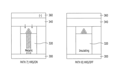
- A ReRAM is fabricated using a method where a stoichiometric transition oxide threshold switching layer and a non-stoichiometric transition metal oxide resistance change layer are formed simultaneously without sequential stacking, with the threshold switching layer comprising stoichiometric oxides like niobium or vanadium oxide, and the resistance change layer formed by oxidizing a part of the electrode, allowing for controlled resistance changes and improved read operations.
Energy Efficiency and Sustainability Aspects of ReRAM
Resistive RAM (ReRAM) represents a significant advancement in semiconductor technology not only for its performance characteristics but also for its impressive energy efficiency profile. When compared to conventional memory technologies like DRAM and flash memory, ReRAM demonstrates substantially lower power consumption during both active operation and standby modes. This energy advantage stems from ReRAM's fundamental operating principle, which requires energy only during state transitions rather than for continuous state maintenance.
The write operations in ReRAM typically consume 10-100 times less energy than equivalent operations in flash memory, while read operations demonstrate similar efficiency improvements. This dramatic reduction in energy requirements makes ReRAM particularly valuable for battery-powered and energy-constrained applications such as IoT devices, wearable technology, and remote sensors where operational longevity is critical.
Beyond direct operational efficiency, ReRAM offers significant sustainability benefits throughout its lifecycle. The manufacturing process for ReRAM requires fewer material inputs and processing steps compared to traditional memory technologies, resulting in reduced resource consumption and manufacturing energy requirements. Many ReRAM designs utilize abundant, non-toxic materials that present fewer environmental concerns than some rare or hazardous elements used in conventional semiconductor manufacturing.
The thermal characteristics of ReRAM further enhance its sustainability profile. With lower heat generation during operation, ReRAM-based systems require less cooling infrastructure, which translates to additional energy savings at the system level. This reduced thermal output also contributes to extended device lifespans by minimizing thermal stress on components.
From a circular economy perspective, ReRAM technologies show promise for improved end-of-life management. The simpler material composition potentially facilitates more effective recycling processes, while the reduced presence of hazardous substances minimizes environmental impact during disposal. These sustainability advantages position ReRAM as an environmentally responsible choice for next-generation memory solutions.
As global computing infrastructure continues to expand, the energy efficiency of memory technologies becomes increasingly critical to overall sustainability goals. ReRAM's favorable energy profile could contribute significantly to reducing the carbon footprint of data centers, edge computing systems, and the billions of connected devices that comprise our digital ecosystem. Industry analysts project that widespread adoption of ReRAM could reduce memory-related energy consumption by 30-50% in certain applications, representing a meaningful contribution to sustainability objectives in the semiconductor industry.
Integration Challenges with Existing Semiconductor Processes
The integration of Resistive RAM (ReRAM) into existing semiconductor manufacturing processes presents significant challenges that must be addressed for successful commercialization. Current CMOS fabrication facilities represent massive investments optimized for conventional memory technologies, making the transition to ReRAM manufacturing economically daunting without compatible integration strategies.
Material compatibility issues stand at the forefront of these challenges. ReRAM devices typically require specialized materials such as metal oxides (HfOx, TaOx) and noble metals that are not standard in traditional CMOS processes. These materials can introduce contamination risks to existing fabrication lines, potentially compromising yield and reliability of both ReRAM and conventional devices manufactured in the same facilities.
Temperature budget constraints further complicate integration efforts. Many ReRAM fabrication steps require high-temperature processing that may exceed the thermal budget limitations of existing CMOS back-end-of-line (BEOL) processes. This thermal incompatibility necessitates careful process engineering to ensure that ReRAM fabrication does not damage underlying CMOS structures or interconnects.
Scaling challenges also emerge when attempting to integrate ReRAM with advanced semiconductor nodes. As conventional semiconductor technology pushes toward smaller feature sizes (5nm and below), integrating ReRAM elements that maintain reliable switching characteristics becomes increasingly difficult. The physical mechanisms underlying resistive switching often require minimum feature dimensions that may not scale proportionally with leading-edge CMOS technology.
Process variability represents another significant hurdle. ReRAM devices exhibit inherent variability in switching parameters, including SET/RESET voltages and resistance states. This variability must be minimized through precise process control to ensure consistent performance across billions of memory cells in a commercial product. Current semiconductor manufacturing processes may require substantial modification to achieve the necessary precision for ReRAM fabrication.
The 3D integration of ReRAM presents both opportunities and challenges. While vertical stacking of ReRAM cells offers tremendous density advantages, it introduces complex fabrication requirements including precise alignment, uniform etching of high-aspect-ratio structures, and effective isolation between layers. These requirements often exceed the capabilities of conventional semiconductor equipment designed primarily for planar device architectures.
Addressing these integration challenges requires collaborative efforts between material scientists, process engineers, and equipment manufacturers. Several approaches show promise, including development of CMOS-compatible ReRAM materials, low-temperature fabrication techniques, and hybrid integration strategies that segregate conventional and ReRAM manufacturing steps to minimize cross-contamination risks.
Unlock deeper insights with PatSnap Eureka Quick Research — get a full tech report to explore trends and direct your research. Try now!
Generate Your Research Report Instantly with AI Agent
Supercharge your innovation with PatSnap Eureka AI Agent Platform!