Resistive RAM in Electronic Standards and Regulations
OCT 9, 202510 MIN READ
Generate Your Research Report Instantly with AI Agent
Patsnap Eureka helps you evaluate technical feasibility & market potential.
ReRAM Technology Background and Objectives
Resistive Random Access Memory (ReRAM) has emerged as a promising non-volatile memory technology that offers significant advantages over conventional memory solutions. The evolution of ReRAM technology can be traced back to the early 2000s when researchers began exploring the potential of resistance switching phenomena in various metal oxide materials. Since then, ReRAM has progressed from a laboratory curiosity to a commercially viable technology with substantial industry interest.
The fundamental operating principle of ReRAM is based on the reversible change in resistance of a dielectric material, typically a metal oxide, under the influence of an applied electric field. This resistance switching behavior enables the storage of binary information, with high and low resistance states representing the '0' and '1' bits. The simplicity of this mechanism contributes to ReRAM's scalability, low power consumption, and fast switching speeds.
The technological trajectory of ReRAM has been characterized by continuous improvements in material composition, device structure, and fabrication processes. Early implementations faced challenges related to reliability, endurance, and uniformity. However, recent advancements have significantly addressed these issues, positioning ReRAM as a competitive alternative to established memory technologies such as NAND flash and DRAM.
In the context of electronic standards and regulations, ReRAM presents unique considerations due to its novel operating mechanisms and integration requirements. The development of standardized testing methodologies, performance metrics, and reliability criteria specific to ReRAM has become increasingly important as the technology matures and approaches widespread adoption.
The primary objectives of ReRAM technology development in relation to electronic standards include establishing uniform characterization methods, defining performance benchmarks, and ensuring compatibility with existing memory interfaces and protocols. Additionally, there is a growing emphasis on addressing regulatory concerns related to material composition, manufacturing processes, and end-of-life management.
From a standardization perspective, key goals include the formulation of industry-wide specifications for ReRAM devices, the development of standardized testing procedures for quality assurance, and the creation of certification frameworks to facilitate market acceptance. These efforts are essential for fostering interoperability and enabling seamless integration of ReRAM into diverse electronic systems.
Looking forward, the technological roadmap for ReRAM encompasses several ambitious targets, including enhanced storage density, improved write/erase endurance, reduced power consumption, and expanded temperature operating ranges. Achieving these objectives will require coordinated efforts across the semiconductor industry, involving material scientists, device engineers, circuit designers, and standardization bodies.
Market Demand Analysis for ReRAM Solutions
The global market for Resistive Random Access Memory (ReRAM) solutions is experiencing significant growth, driven by increasing demands for advanced non-volatile memory technologies that overcome the limitations of traditional storage solutions. Current market analysis indicates that the ReRAM market is projected to grow at a compound annual growth rate of over 16% during the forecast period 2023-2030, with the market value expected to reach approximately 1.2 billion USD by 2030.
The primary market demand for ReRAM stems from its unique value proposition in addressing the memory-storage gap in modern computing architectures. With data-intensive applications becoming increasingly prevalent across various industries, there is a growing need for memory solutions that combine the speed of DRAM with the non-volatility of flash storage. ReRAM's ability to offer fast read/write speeds, low power consumption, and high endurance positions it as an ideal candidate for next-generation memory systems.
Several key industry verticals are driving the demand for ReRAM solutions. The consumer electronics sector represents a significant market segment, with applications in smartphones, tablets, and wearable devices where power efficiency and performance are critical. The automotive industry is another major demand driver, particularly with the rise of autonomous vehicles and advanced driver-assistance systems that require reliable, high-performance memory for real-time data processing and storage.
Enterprise storage systems and data centers are increasingly looking toward ReRAM as a solution for improving system performance while reducing power consumption. The technology's potential to enable in-memory computing and reduce data movement between storage and processing units aligns well with the industry's focus on energy efficiency and computational speed.
The Internet of Things (IoT) ecosystem presents perhaps the most promising growth opportunity for ReRAM. The proliferation of edge devices requiring low-power, high-reliability memory solutions has created a substantial market need that ReRAM is well-positioned to address. Industry analysts predict that by 2025, over 75 billion IoT devices will be connected worldwide, creating an enormous potential market for embedded ReRAM solutions.
Geographically, the Asia-Pacific region dominates the ReRAM market, accounting for approximately 45% of global demand, followed by North America and Europe. This regional distribution reflects the concentration of semiconductor manufacturing capabilities and the presence of major technology companies driving innovation in memory technologies.
Despite the promising market outlook, widespread adoption of ReRAM faces challenges related to standardization and regulatory compliance. The lack of unified standards for ReRAM implementation and testing protocols has created market fragmentation, slowing adoption rates in conservative sectors such as healthcare and industrial automation where regulatory compliance is paramount.
ReRAM Development Status and Technical Challenges
Resistive RAM (ReRAM) technology has evolved significantly over the past decade, yet still faces substantial technical challenges that impede its widespread commercial adoption. Currently, ReRAM exists in a transitional state between promising laboratory demonstrations and full-scale industrial implementation. The global ReRAM market, valued at approximately $310 million in 2022, is projected to grow at a CAGR of 16% through 2030, indicating strong industry interest despite technical limitations.
The fundamental operational principle of ReRAM—resistance switching through the formation and rupture of conductive filaments—has been well-established. However, significant variability in switching behavior remains a critical challenge. Device-to-device and cycle-to-cycle variations often exceed 20%, substantially higher than the <5% typically required for reliable commercial memory applications. This inconsistency manifests in unpredictable set/reset voltages and resistance states, complicating circuit design and limiting yield rates.
Endurance limitations represent another major technical hurdle. While conventional flash memory achieves 10^5 write cycles, and DRAM exceeds 10^16 cycles, current ReRAM devices typically demonstrate only 10^6 to 10^9 cycles before performance degradation. This limitation stems from structural degradation of the switching layer during repeated programming operations, resulting in retention failures and resistance drift over time.
Power consumption during the forming process remains problematic, with forming voltages often exceeding 3V—significantly higher than desired for low-power applications. This initial high-voltage requirement complicates integration with standard CMOS processes and increases peripheral circuit complexity. Additionally, the sneak current issue in crossbar arrays continues to challenge large-scale integration efforts, necessitating selector devices that add complexity and cost.
Material stability presents ongoing challenges, particularly regarding temperature sensitivity and oxygen vacancy migration. Many ReRAM devices exhibit accelerated degradation at elevated temperatures (>85°C), limiting their applicability in automotive and industrial environments. The industry has yet to standardize on optimal material stacks, with competing approaches using HfOx, TaOx, and various transition metal oxides each presenting unique trade-offs between performance metrics.
Scaling capabilities, while theoretically promising down to sub-10nm nodes, face practical fabrication challenges. As cell dimensions decrease, the statistical nature of filament formation becomes increasingly problematic, resulting in higher variability. Current manufacturing processes struggle to maintain consistent film quality and interface characteristics at these dimensions.
From a geographical perspective, ReRAM development exhibits regional specialization. Asian manufacturers (particularly in Japan, South Korea, and Taiwan) lead in production-oriented research, while North American and European institutions focus more on novel materials and theoretical advancements. This distribution creates both collaboration opportunities and intellectual property challenges for global standardization efforts.
Current ReRAM Implementation Approaches
01 Resistive RAM structure and materials
Resistive RAM (RRAM) devices are constructed with specific materials and structures to enable resistive switching behavior. These typically include a metal-insulator-metal (MIM) structure where the insulator layer can be made of various materials such as metal oxides, chalcogenides, or perovskites. The choice of materials significantly affects the performance characteristics including switching speed, endurance, and retention time. Different electrode materials and interface engineering techniques are employed to optimize the resistive switching mechanism.- Resistive RAM device structures: Resistive RAM (RRAM) devices are typically structured with a resistive switching material sandwiched between two electrodes. Various materials can be used for the resistive switching layer, including metal oxides, chalcogenides, and perovskites. The device structure can be optimized by controlling the thickness of the switching layer, electrode materials, and interface properties to improve performance characteristics such as switching speed, endurance, and retention time.
- Switching mechanisms in RRAM: The resistive switching mechanism in RRAM involves the formation and rupture of conductive filaments within the resistive switching material. This process can be controlled by applying appropriate voltage pulses to induce SET (low resistance state) and RESET (high resistance state) operations. Different types of switching mechanisms exist, including filamentary switching, interface-type switching, and valence change mechanisms, each offering unique advantages for specific applications.
- RRAM fabrication techniques: Advanced fabrication techniques for RRAM include atomic layer deposition, sputtering, and sol-gel methods to create high-quality resistive switching layers. Integration with CMOS technology requires careful consideration of thermal budgets and material compatibility. Novel approaches such as 3D stacking and crossbar architectures enable high-density memory arrays, while techniques like doping and interface engineering can enhance device performance and reliability.
- RRAM materials innovation: Material innovations for RRAM include various metal oxides (HfOx, TaOx, TiOx), complex oxides, and two-dimensional materials. Each material system offers different advantages in terms of switching characteristics, retention, and endurance. Multilayer structures combining different materials can provide enhanced performance by leveraging complementary properties. Emerging materials such as organic compounds and polymer-based resistive switching elements are also being explored for flexible and biocompatible memory applications.
- RRAM circuit design and applications: Circuit designs for RRAM include sensing amplifiers, write drivers, and address decoders optimized for the unique characteristics of resistive switching. These circuits must address challenges such as sneak path currents in crossbar arrays and variability in device parameters. RRAM applications extend beyond conventional memory to include neuromorphic computing, in-memory computing, and security applications like physical unclonable functions (PUFs). The non-volatile nature and analog switching capabilities make RRAM particularly suitable for edge AI and IoT applications where power efficiency is critical.
02 Resistive switching mechanisms and operation
The operation of resistive RAM relies on different switching mechanisms that change the resistance state of the memory cell. These mechanisms include filamentary conduction, interface-type switching, and phase change processes. The switching can be controlled by applying appropriate voltage pulses that create or rupture conductive filaments within the switching layer. Understanding these mechanisms is crucial for designing reliable RRAM devices with consistent performance characteristics and addressing issues like variability and endurance degradation.Expand Specific Solutions03 Integration and fabrication techniques
Advanced fabrication techniques are essential for integrating resistive RAM into existing semiconductor manufacturing processes. These include methods for depositing uniform switching layers, creating precise electrode structures, and ensuring compatibility with CMOS technology. Various approaches such as atomic layer deposition, physical vapor deposition, and chemical vapor deposition are used to create high-quality films. 3D integration techniques are also employed to increase memory density and improve overall system performance.Expand Specific Solutions04 Circuit design and memory architecture
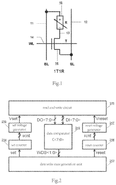
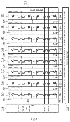
Specialized circuit designs and memory architectures are developed to address the unique characteristics of resistive RAM. These include sense amplifiers for reading the resistance states, write drivers for programming operations, and control circuits for managing the memory array. Cross-point arrays, 1T1R (one transistor, one resistor) configurations, and 3D stacking architectures are common approaches to organizing RRAM cells. These designs aim to maximize density while minimizing issues like sneak path currents and read/write disturbances.Expand Specific Solutions05 Applications and emerging technologies
Resistive RAM is being developed for various applications beyond conventional memory storage. These include neuromorphic computing where RRAM cells mimic synaptic behavior, in-memory computing to reduce data movement, and security applications like physical unclonable functions. RRAM is also being explored for use in harsh environments due to its radiation hardness and temperature stability. Hybrid systems combining RRAM with other memory technologies are being developed to leverage the strengths of each technology while mitigating their weaknesses.Expand Specific Solutions
Key Industry Players in ReRAM Development
The Resistive RAM (ReRAM) market is currently in a growth phase, with increasing adoption across various electronic applications. The market size is projected to expand significantly due to ReRAM's advantages in power efficiency and data retention. From a technical maturity perspective, major players like Samsung Electronics, Taiwan Semiconductor Manufacturing Co., and Fujitsu have made substantial progress in standardizing ReRAM technologies. Companies including Winbond Electronics, Macronix, and Rambus are actively developing compliance frameworks for ReRAM integration into existing electronic standards. Meanwhile, research institutions such as Bar-Ilan University and the Institute of Microelectronics of Chinese Academy of Sciences are collaborating with industry leaders like IBM and Sharp to address regulatory challenges related to reliability, endurance, and compatibility with international electronic standards, positioning ReRAM as a promising next-generation memory technology.
Samsung Electronics Co., Ltd.
Technical Solution: Samsung has developed comprehensive ReRAM technology that complies with JEDEC standards for non-volatile memory. Their approach focuses on cross-point array architecture that enables high-density storage while maintaining compatibility with existing semiconductor manufacturing processes. Samsung's ReRAM solutions incorporate advanced materials engineering with hafnium oxide-based switching layers that demonstrate excellent retention characteristics and endurance cycles exceeding 10^6. The company has actively participated in establishing industry standards through JEDEC's JC-42.4 Committee on Nonvolatile Memory and has implemented ISO/IEC 27001 information security standards in their ReRAM development process. Samsung's ReRAM technology addresses both consumer electronics requirements (IEC 62368) and automotive standards (AEC-Q100), positioning their solutions for broad market adoption.
Strengths: Extensive manufacturing infrastructure allows for rapid scaling and standardization; strong position in memory market provides leverage for establishing new standards. Weaknesses: Relatively higher power consumption compared to some competitors' solutions; integration challenges with existing memory hierarchies.
Taiwan Semiconductor Manufacturing Co., Ltd.
Technical Solution: TSMC has developed an advanced ReRAM manufacturing platform that integrates seamlessly with their standard CMOS process nodes, ensuring compatibility with existing semiconductor standards. Their approach focuses on back-end-of-line (BEOL) integration that minimizes disruption to established manufacturing workflows while meeting IPC-A-610 electronics assembly standards. TSMC's ReRAM technology features a hafnium oxide-based switching layer with titanium nitride electrodes that demonstrates excellent uniformity across wafers, addressing key manufacturing variability concerns highlighted in JEDEC standards. The company has implemented comprehensive reliability testing protocols aligned with JEDEC JESD22 environmental standards and JESD47 stress test qualifications. TSMC has also developed specialized electrostatic discharge (ESD) protection schemes for their ReRAM devices that comply with IEC 61000-4-2 standards, ensuring robustness in various application environments. Their foundry approach enables customers to implement ReRAM solutions that can be certified to application-specific standards ranging from consumer electronics to automotive and medical devices.
Strengths: Unparalleled manufacturing expertise and capacity; ability to integrate ReRAM with diverse logic processes. Weaknesses: Relies on partners for complete memory subsystem design; less vertical integration compared to IDMs.
Critical ReRAM Patents and Technical Innovations
Resistive RAM, method for fabricating the same, and method for driving the same
PatentActiveUS9214631B2
Innovation
- A ReRAM is fabricated using a method where a stoichiometric transition oxide threshold switching layer and a non-stoichiometric transition metal oxide resistance change layer are formed simultaneously without sequential stacking, with the threshold switching layer comprising stoichiometric oxides like niobium or vanadium oxide, and the resistance change layer formed by oxidizing a part of the electrode, allowing for controlled resistance changes and improved read operations.
Storage array programming method and device for resistive random access memory
PatentActiveUS10522221B2
Innovation
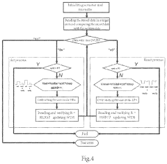
- A storage array programming method and device that reads current data, compares it bit-by-bit with the data to be written, generates a data write state, and performs set or reset operations only on units where data is inconsistent, using counters to limit voltage pulses and avoid repetitive writing, thereby ensuring only necessary units are written, reducing interference and power consumption.
Regulatory Framework for ReRAM Technologies
The regulatory landscape for Resistive Random Access Memory (ReRAM) technologies is evolving rapidly as this emerging non-volatile memory solution gains traction in commercial applications. Current regulatory frameworks primarily address ReRAM through broader semiconductor and electronic component standards rather than through ReRAM-specific regulations. Organizations such as the International Electrotechnical Commission (IEC), JEDEC Solid State Technology Association, and IEEE play crucial roles in developing these standards.
The IEC has established several standards relevant to ReRAM implementation, including IEC 62830 series for semiconductor devices and IEC 61000 for electromagnetic compatibility requirements. These standards ensure ReRAM devices maintain operational integrity when integrated into larger electronic systems. JEDEC, meanwhile, has developed JEP122G guidelines for reliability qualification of semiconductor products that manufacturers must consider when bringing ReRAM solutions to market.
Safety certification represents another critical regulatory dimension for ReRAM technologies. Underwriters Laboratories (UL) and the International Organization for Standardization (ISO) have established safety standards that ReRAM devices must meet before commercial deployment. These include UL 60950 for information technology equipment and ISO/IEC 27001 for information security management systems when ReRAM is used in data storage applications.
Environmental regulations significantly impact ReRAM manufacturing and end-of-life management. The European Union's Restriction of Hazardous Substances (RoHS) directive and Registration, Evaluation, Authorization and Restriction of Chemicals (REACH) regulation impose strict limitations on materials used in electronic components. ReRAM developers must ensure compliance with these regulations by carefully selecting materials and manufacturing processes that minimize environmental impact.
Data security and privacy regulations present additional compliance challenges for ReRAM technologies, particularly in applications involving sensitive information storage. The General Data Protection Regulation (GDPR) in Europe and similar regulations worldwide establish requirements for data protection that ReRAM-based storage solutions must address through appropriate encryption and access control mechanisms.
Regional variations in regulatory approaches create complexity for global ReRAM deployment. While the European Union maintains stringent environmental and safety standards, the United States focuses more on performance specifications through NIST guidelines. Asian markets, particularly Japan and South Korea, have developed specialized frameworks for memory technologies that incorporate ReRAM-specific considerations.
As ReRAM technology matures, regulatory frameworks will likely evolve to address its unique characteristics more directly. Industry stakeholders are actively participating in standards development organizations to ensure emerging regulations balance innovation enablement with necessary safety and compatibility requirements.
Environmental Impact of ReRAM Manufacturing
The manufacturing processes for Resistive Random Access Memory (ReRAM) present both environmental challenges and opportunities compared to conventional memory technologies. ReRAM fabrication typically involves fewer process steps than traditional NAND flash memory, potentially reducing the overall energy consumption and chemical usage in manufacturing. Studies indicate that ReRAM production can achieve up to 30% reduction in carbon footprint compared to equivalent DRAM or flash memory manufacturing processes.
However, ReRAM manufacturing still utilizes various heavy metals and rare earth elements that pose environmental concerns. The deposition of metal oxide layers often requires precursors containing ruthenium, hafnium, or tantalum - materials whose extraction involves significant environmental disruption including habitat destruction, water pollution, and high energy consumption. The semiconductor industry's typical water usage rates of 4-10 million gallons per day also apply to ReRAM fabrication facilities.
Waste management represents another critical environmental consideration. The etching processes used in ReRAM manufacturing generate hazardous byproducts including perfluorinated compounds (PFCs) and nitrogen trifluoride (NF3), which are potent greenhouse gases with global warming potentials thousands of times greater than CO2. Current abatement technologies can capture approximately 90% of these emissions, but the remaining 10% continues to contribute to climate change.
Several leading ReRAM manufacturers have implemented sustainability initiatives to address these concerns. These include closed-loop water recycling systems that reduce freshwater consumption by up to 80%, energy efficiency improvements in clean room operations, and chemical recovery systems that minimize waste. The industry is also exploring alternative materials with lower environmental impacts, such as zinc-oxide based switching layers that could replace more environmentally problematic materials.
Life cycle assessments comparing ReRAM to conventional memory technologies suggest that despite manufacturing challenges, ReRAM's lower operational power requirements and longer potential lifespan may offset initial environmental impacts over the product lifetime. The non-volatile nature of ReRAM eliminates the need for constant power to maintain stored data, potentially reducing the carbon footprint of data centers by 15-20% if widely adopted.
As environmental regulations become increasingly stringent worldwide, ReRAM manufacturers face growing pressure to comply with directives such as the EU's Restriction of Hazardous Substances (RoHS), Registration, Evaluation, Authorization and Restriction of Chemicals (REACH), and various electronic waste management protocols. These regulatory frameworks will likely shape future ReRAM manufacturing processes toward greater sustainability.
Unlock deeper insights with Patsnap Eureka Quick Research — get a full tech report to explore trends and direct your research. Try now!
Generate Your Research Report Instantly with AI Agent
Supercharge your innovation with Patsnap Eureka AI Agent Platform!