Research on Electrode Kinetics in Resistive RAM Devices
OCT 9, 20259 MIN READ
Generate Your Research Report Instantly with AI Agent
Patsnap Eureka helps you evaluate technical feasibility & market potential.
Resistive RAM Electrode Kinetics Background and Objectives
Resistive Random Access Memory (RRAM) has emerged as a promising candidate for next-generation non-volatile memory technologies due to its simple structure, high scalability, low power consumption, and compatibility with CMOS processes. The evolution of RRAM technology can be traced back to the 1960s when researchers first observed resistive switching phenomena in metal oxides. However, significant progress in understanding and developing RRAM devices has only been achieved in the past two decades, driven by the increasing demand for high-density, high-speed, and low-power memory solutions.
The fundamental operating principle of RRAM relies on the formation and rupture of conductive filaments within a dielectric layer sandwiched between two electrodes. This process, known as resistive switching, allows the device to toggle between high resistance state (HRS) and low resistance state (LRS), corresponding to the binary "0" and "1" states in digital memory applications. The electrode kinetics, which involves the interaction between electrode materials and the dielectric layer, plays a crucial role in determining the performance, reliability, and endurance of RRAM devices.
Recent technological trends in RRAM research have focused on optimizing electrode materials and interfaces to enhance device performance. Various electrode materials, including noble metals (Pt, Au), transition metals (Ti, Cu, Ag), and metal nitrides (TiN, TaN), have been investigated to understand their impact on resistive switching behaviors. The electrode-dielectric interface has been recognized as a critical factor affecting the formation and stability of conductive filaments, thus directly influencing the switching characteristics and reliability of RRAM devices.
The primary technical objectives of electrode kinetics research in RRAM include: understanding the fundamental mechanisms of ion migration and redox reactions at the electrode-dielectric interface; developing models to predict and control filament formation and dissolution processes; optimizing electrode materials and structures to enhance switching speed, endurance, and retention; and addressing reliability issues such as variability, sneak path problems, and resistance drift.
Furthermore, electrode kinetics research aims to enable multi-level cell (MLC) operations by precisely controlling the filament dimensions and resistance states. This capability is essential for increasing storage density and implementing neuromorphic computing applications, where RRAM devices can serve as artificial synapses with analog-like behavior. The ultimate goal is to develop RRAM technology that can meet the stringent requirements of both conventional memory applications and emerging computing paradigms.
Understanding electrode kinetics is also crucial for scaling RRAM devices to sub-10 nm dimensions while maintaining reliable operation. As device dimensions shrink, the influence of interfaces becomes increasingly dominant, making electrode engineering a key factor in realizing high-density RRAM arrays for future memory and computing systems.
Market Analysis for ReRAM Technology Applications
The global ReRAM (Resistive Random Access Memory) market is experiencing significant growth, with projections indicating an expansion from $1.2 billion in 2023 to approximately $4.6 billion by 2028, representing a compound annual growth rate (CAGR) of 30.8%. This remarkable growth trajectory is primarily driven by increasing demand for high-performance, energy-efficient memory solutions across various sectors.
The consumer electronics segment currently dominates the ReRAM market, accounting for nearly 40% of total market share. Smartphones, tablets, and wearable devices are increasingly incorporating ReRAM technology due to its low power consumption and fast switching speeds. Industry analysts predict that by 2026, over 15% of premium smartphones will feature some form of ReRAM components.
Enterprise storage systems represent another substantial market segment, valued at approximately $310 million in 2023. The need for faster data processing and reduced latency in data centers is propelling adoption in this sector, with projections suggesting a 35% annual growth rate through 2027. Cloud service providers are particularly interested in ReRAM's potential to reduce energy consumption in data centers by up to 30% compared to conventional memory technologies.
The automotive industry is emerging as a promising growth area for ReRAM applications. Advanced driver-assistance systems (ADAS) and autonomous vehicles require memory solutions that can operate reliably under extreme conditions while processing vast amounts of sensor data with minimal latency. This segment is expected to grow at 42% annually, reaching $680 million by 2028.
Industrial IoT applications represent another expanding market for ReRAM technology. The ability to perform in-memory computing and edge processing makes ReRAM particularly valuable for industrial sensors and monitoring systems. Market research indicates this segment will grow from $220 million in 2023 to over $900 million by 2028.
Regionally, North America currently leads the ReRAM market with approximately 38% share, followed by Asia-Pacific at 35% and Europe at 22%. However, the Asia-Pacific region is expected to demonstrate the fastest growth rate at 34% annually, driven by extensive manufacturing capabilities and increasing adoption in consumer electronics.
Key market challenges include competition from alternative emerging memory technologies such as MRAM and PCM, as well as the need for further improvements in reliability and endurance for certain applications. Despite these challenges, the unique combination of non-volatility, low power consumption, and high-speed operation positions ReRAM favorably in the competitive memory landscape, particularly as electrode kinetics research advances to address current limitations.
Current Challenges in Electrode Kinetics for ReRAM
Despite significant advancements in ReRAM technology, electrode kinetics remains one of the most challenging aspects limiting device performance and reliability. The electrode-oxide interface plays a crucial role in the switching mechanism, yet understanding and controlling the complex electrochemical reactions at this interface continues to be problematic. Current challenges primarily revolve around the inconsistent switching behavior caused by variations in electrode material properties and interface conditions.
A major obstacle is the lack of comprehensive in-situ characterization techniques capable of monitoring electrode kinetics during actual device operation. Most analytical methods provide only static or post-operation information, failing to capture the dynamic processes occurring during switching events. This limitation significantly hampers the development of accurate models for electrode behavior under various operational conditions.
The electrode material selection presents another significant challenge. Noble metals like Pt and Au offer excellent stability but suffer from poor adhesion to oxide layers and higher fabrication costs. Conversely, reactive metals such as Ti and Ta provide better adhesion but introduce additional complexity through the formation of interfacial oxide layers that can unpredictably alter device characteristics.
Interface degradation mechanisms remain poorly understood, particularly how repeated cycling affects the electrode-oxide interface at the atomic level. Current research indicates that ion migration, electromigration, and localized Joule heating contribute to progressive changes in interface properties, but quantifying these effects and developing mitigation strategies has proven difficult.
The scaling behavior of electrode kinetics presents additional complications. As device dimensions shrink below 40nm, quantum effects and surface energy considerations begin to dominate, significantly altering electrode behavior compared to larger devices. This scaling discrepancy creates challenges in translating laboratory results to commercially viable technologies.
Variability in switching parameters represents perhaps the most pressing challenge for commercial applications. Device-to-device and cycle-to-cycle variations in switching voltages, currents, and resistance states are frequently attributed to stochastic processes at the electrode-oxide interface, yet controlling these variations remains elusive despite extensive research efforts.
Temperature dependence of electrode kinetics further complicates matters, with switching behavior showing significant variations across operating temperature ranges. This temperature sensitivity impacts both performance and reliability, creating additional design constraints for practical applications in environments with fluctuating thermal conditions.
Current Electrode Material Solutions and Interfaces
01 Electrode materials and composition for RRAM devices
The choice of electrode materials significantly impacts the performance of resistive RAM devices. Various materials such as noble metals, transition metals, and metal oxides can be used as electrodes to control the kinetics of resistive switching. The composition of these electrodes affects parameters like switching speed, endurance, and retention. Optimizing electrode composition can enhance the formation and rupture of conductive filaments, which is crucial for reliable RRAM operation.- Electrode materials and composition for ReRAM devices: The choice of electrode materials significantly impacts the performance of resistive RAM devices. Various materials such as metal oxides, noble metals, and conductive polymers can be used as electrodes to control the kinetics of resistive switching. The composition of these electrodes affects parameters like switching speed, retention time, and endurance. Optimizing electrode composition can enhance the formation and rupture of conductive filaments, which is crucial for reliable resistive switching operations.
- Interface engineering for improved switching kinetics: Engineering the interface between the electrode and the switching layer is critical for controlling electrode kinetics in ReRAM devices. Techniques such as inserting buffer layers, surface treatments, and creating specific interface structures can modify the ion migration pathways and redox reactions at the electrode-switching layer interface. These modifications can lead to more controlled and efficient resistive switching, reduced variability, and improved device reliability by optimizing the kinetics of filament formation and dissolution.
- Oxygen vacancy dynamics and ion migration control: The movement of oxygen vacancies and ions between electrodes plays a fundamental role in the switching mechanism of ReRAM devices. Controlling the kinetics of these migrations through electrode design, applied voltage profiles, and temperature management can significantly enhance device performance. Strategies include creating oxygen reservoirs within electrodes, designing electrodes with specific oxygen affinity, and implementing pulse schemes that regulate ion movement during switching operations to achieve more reliable and faster resistive switching.
- Multi-layer electrode structures for enhanced performance: Multi-layer electrode structures can be designed to optimize the electrode kinetics in ReRAM devices. By combining different materials with complementary properties, these structures can provide better control over the resistive switching process. For example, a composite electrode might include a layer for adhesion, another for controlling ion migration, and a third for electrical conductivity. This approach allows for fine-tuning of the electrode-switching layer interaction, resulting in improved switching speed, endurance, and reliability.
- Temperature effects on electrode kinetics: Temperature significantly influences the electrode kinetics in ReRAM devices by affecting ion mobility, diffusion rates, and chemical reactions at the electrode interfaces. Understanding and controlling these temperature-dependent processes is crucial for reliable device operation. Techniques such as localized heating elements, thermal management structures, and temperature-compensated operation protocols can be implemented to optimize the electrode kinetics across different operating conditions, ensuring consistent performance and extending device lifetime.
02 Interface engineering for improved switching kinetics
Engineering the interface between the electrode and the switching layer is critical for controlling electrode kinetics in RRAM devices. Techniques such as inserting buffer layers, modifying surface properties, and creating engineered defects at the interface can significantly improve switching behavior. These modifications affect the ion migration process and filament formation dynamics, leading to enhanced switching speed, reduced variability, and lower operating voltages.Expand Specific Solutions03 Oxygen vacancy dynamics and ion migration control
The movement of oxygen vacancies and ions at the electrode interface plays a crucial role in the switching mechanism of RRAM devices. Controlling these dynamics through electrode design can significantly impact device performance. Strategies include using oxygen scavenging electrodes, creating oxygen reservoirs, and engineering the oxygen affinity of electrode materials. These approaches help regulate the formation and dissolution of conductive filaments, improving switching reliability and endurance.Expand Specific Solutions04 Novel electrode structures and architectures
Innovative electrode structures and device architectures can enhance the electrode kinetics in RRAM devices. These include multi-layer electrodes, nanostructured electrodes, and three-dimensional electrode configurations. Such designs provide better control over the switching region, improve current distribution, and enhance the overall switching performance. Advanced fabrication techniques enable precise control over electrode geometry and structure, leading to more reliable and efficient RRAM devices.Expand Specific Solutions05 Temperature and field effects on electrode kinetics
Temperature and electric field significantly influence electrode kinetics in RRAM devices. Understanding and controlling these effects is essential for optimizing device performance. Techniques such as thermal management, pulse engineering, and field confinement can be employed to regulate the switching process. These approaches help in controlling the rate of ion migration, filament growth, and dissolution, leading to improved switching speed, endurance, and reliability under various operating conditions.Expand Specific Solutions
Key Industry Players in ReRAM Development
The resistive RAM (RRAM) electrode kinetics research field is currently in a growth phase, with market projections showing significant expansion as memory technologies evolve beyond traditional NAND and DRAM. Major semiconductor manufacturers including Micron Technology, Samsung Electronics, and KIOXIA are investing heavily in this technology, while specialized players like Weebit Nano and Unisantis Electronics are developing innovative approaches to overcome technical challenges. Research institutions such as Fudan University and GIST collaborate with industry leaders like IBM and Fujitsu to address fundamental electrode kinetics issues. The technology is approaching commercial maturity, with companies like TSMC and UMC providing manufacturing capabilities, though challenges in reliability, endurance, and scaling still require significant research investment before widespread adoption.
Micron Technology, Inc.
Technical Solution: Micron has developed advanced electrode materials and interface engineering techniques for ReRAM devices. Their research focuses on optimizing the electrode-oxide interface to enhance switching performance and reliability. Micron's approach involves using noble metal electrodes (such as Pt, Ru) combined with oxygen exchange layers to control oxygen vacancy formation and migration[1]. They've implemented a multi-layer electrode structure that creates an oxygen reservoir effect, facilitating controlled redox reactions at the electrode-oxide interface. Their research demonstrates that electrode kinetics can be significantly improved by engineering the work function difference between top and bottom electrodes, resulting in more uniform filament formation and dissolution[3]. Micron has also explored doping strategies for electrode materials to catalyze the redox reactions responsible for resistive switching.
Strengths: Superior control over oxygen vacancy dynamics through engineered electrode interfaces; excellent retention characteristics; reduced variability in switching parameters. Weaknesses: Higher manufacturing complexity due to multi-layer electrode structures; potential material compatibility issues with standard CMOS processes; increased production costs compared to simpler electrode configurations.
International Business Machines Corp.
Technical Solution: IBM has conducted extensive research on electrode kinetics in ReRAM, focusing on phase-change mechanisms and interface phenomena. Their approach centers on understanding the fundamental physics of electrode-oxide interactions through advanced characterization techniques including in-situ TEM and spectroscopic analysis[1]. IBM has developed proprietary electrode materials with tailored work functions to optimize charge transfer at the metal-oxide interface. Their research demonstrates that electrode surface treatment and crystallographic orientation significantly impact filament nucleation and growth kinetics[3]. IBM's electrode engineering includes atomic layer deposition of transition metal electrodes with precisely controlled oxygen affinity gradients. They've pioneered the concept of "kinetic balancing" where electrode properties are matched to specific switching oxide requirements for optimized performance. Recent publications highlight their work on electrode-induced strain effects that can modulate oxygen vacancy mobility and consequently control switching characteristics[6]. IBM has also explored the use of 2D materials as electrode interlayers to enhance interface stability.
Strengths: Fundamental understanding of electrode-oxide interface physics; excellent control over filament morphology; superior retention characteristics at elevated temperatures. Weaknesses: More complex fabrication requirements; higher development costs; challenges in scaling some of their electrode engineering approaches to high-volume manufacturing.
Critical Patents and Research on ReRAM Electrode Kinetics
Resistive random access memory device
PatentActiveUS20180040816A1
Innovation
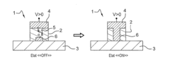
- A metal oxide-based CBRAM memory cell is developed, incorporating a transition metal from groups 3, 4, 5, or 6 and a chalcogen element, with an interface layer that creates oxygen vacancies, facilitating the formation of conductive filaments and enhancing their retention by acting as a barrier against filament dissolution.
Resistive random access memory device
PatentActiveUS20150280120A1
Innovation
- A CBRAM memory cell with a solid electrolyte comprising a region of doped metal oxide, where the second metal reduces the band gap energy, facilitating the formation of conductive filaments by creating oxygen vacancies, thereby reducing the forming voltage and improving electrical performances.
Materials Science Considerations for ReRAM Electrodes
The selection of electrode materials in Resistive Random Access Memory (ReRAM) devices represents a critical factor that significantly influences device performance, reliability, and scalability. Electrode materials must satisfy multiple requirements including excellent electrical conductivity, appropriate work function, chemical stability, and compatibility with standard semiconductor manufacturing processes. The electrode-oxide interface plays a fundamental role in the formation and rupture of conductive filaments that underpin ReRAM switching mechanisms.
Noble metals such as platinum (Pt), gold (Au), and ruthenium (Ru) have been extensively investigated as inert electrode materials due to their excellent chemical stability and resistance to oxidation. These properties ensure minimal electrode degradation during operation and contribute to device longevity. However, cost considerations and integration challenges with CMOS technology have prompted research into alternative electrode materials.
Transition metals and their nitrides, including titanium nitride (TiN), tantalum nitride (TaN), and tungsten nitride (WN), have emerged as promising electrode candidates. These materials offer favorable work functions, good electrical conductivity, and superior diffusion barrier properties that prevent metal ion migration into the switching layer. Additionally, their compatibility with standard semiconductor fabrication processes makes them particularly attractive for commercial applications.
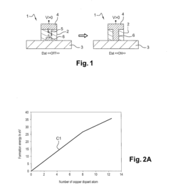
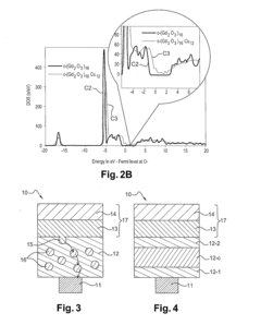
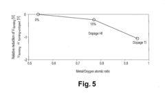
The physical and chemical interactions at the electrode-oxide interface critically determine the formation energy and spatial distribution of oxygen vacancies, which constitute the primary defects responsible for conductive filament formation. Recent studies have demonstrated that engineering the roughness and crystallographic orientation of electrode surfaces can effectively modulate filament formation dynamics and switching variability.
Electrode thickness represents another important parameter affecting ReRAM performance. Ultrathin electrodes may enhance electric field concentration and reduce operating voltages, but potentially compromise device reliability. Conversely, thicker electrodes provide better mechanical stability and heat dissipation capabilities at the expense of increased fabrication complexity and potentially higher operating voltages.
Advanced electrode architectures incorporating multilayer structures or nanocomposites have shown promise in addressing the trade-offs between different performance metrics. For instance, bilayer electrodes combining an adhesion-promoting layer with a highly conductive cap layer can simultaneously enhance interface quality and electrical performance. Similarly, nanostructured electrodes with controlled porosity can facilitate ion migration while maintaining structural integrity during cycling.
Noble metals such as platinum (Pt), gold (Au), and ruthenium (Ru) have been extensively investigated as inert electrode materials due to their excellent chemical stability and resistance to oxidation. These properties ensure minimal electrode degradation during operation and contribute to device longevity. However, cost considerations and integration challenges with CMOS technology have prompted research into alternative electrode materials.
Transition metals and their nitrides, including titanium nitride (TiN), tantalum nitride (TaN), and tungsten nitride (WN), have emerged as promising electrode candidates. These materials offer favorable work functions, good electrical conductivity, and superior diffusion barrier properties that prevent metal ion migration into the switching layer. Additionally, their compatibility with standard semiconductor fabrication processes makes them particularly attractive for commercial applications.
The physical and chemical interactions at the electrode-oxide interface critically determine the formation energy and spatial distribution of oxygen vacancies, which constitute the primary defects responsible for conductive filament formation. Recent studies have demonstrated that engineering the roughness and crystallographic orientation of electrode surfaces can effectively modulate filament formation dynamics and switching variability.
Electrode thickness represents another important parameter affecting ReRAM performance. Ultrathin electrodes may enhance electric field concentration and reduce operating voltages, but potentially compromise device reliability. Conversely, thicker electrodes provide better mechanical stability and heat dissipation capabilities at the expense of increased fabrication complexity and potentially higher operating voltages.
Advanced electrode architectures incorporating multilayer structures or nanocomposites have shown promise in addressing the trade-offs between different performance metrics. For instance, bilayer electrodes combining an adhesion-promoting layer with a highly conductive cap layer can simultaneously enhance interface quality and electrical performance. Similarly, nanostructured electrodes with controlled porosity can facilitate ion migration while maintaining structural integrity during cycling.
Reliability and Endurance Testing Methodologies
Reliability and endurance testing methodologies for Resistive RAM (RRAM) devices are critical for evaluating their long-term performance and commercial viability. These methodologies typically involve accelerated stress tests that simulate years of operation within a compressed timeframe. The most common approach is the pulse endurance test, where devices undergo repeated SET/RESET operations until failure, with performance metrics monitored throughout the process.
Standard testing protocols include the application of constant voltage stress (CVS) and constant current stress (CCS) to evaluate how electrode kinetics influence device degradation over time. These tests are typically performed at elevated temperatures (85°C to 125°C) to accelerate failure mechanisms while monitoring resistance states after each programming cycle. The retention capability is assessed through high-temperature bake tests, where devices are stored at elevated temperatures (typically 85°C to 150°C) for extended periods while periodically measuring their resistance states.
Statistical analysis plays a crucial role in reliability assessment, with Weibull distribution commonly used to model failure rates and predict device lifetimes. The characteristic lifetime (T63.2) and Weibull slope (β) provide insights into failure mechanisms and their uniformity across device populations. Advanced testing methodologies incorporate in-situ monitoring techniques that capture real-time changes in electrode interfaces during cycling, revealing how ion migration and redox reactions evolve with repeated operations.
Specialized test structures, including cross-point arrays and dedicated test vehicles with varying electrode materials and geometries, enable comparative studies of electrode kinetics under identical stress conditions. These structures help isolate the impact of electrode materials on reliability by controlling other variables in the device architecture.
Recent advancements in reliability testing include the implementation of variable pulse width and amplitude schemes that more accurately reflect real-world operating conditions. These tests reveal how electrode kinetics respond to different programming conditions and help establish optimal operating windows that balance performance with longevity. Additionally, noise analysis techniques such as random telegraph noise (RTN) and low-frequency noise measurements provide insights into the microscopic processes occurring at electrode interfaces during cycling.
The correlation between accelerated testing and actual field performance remains a significant challenge, necessitating the development of physics-based models that connect electrode kinetics to failure mechanisms. These models increasingly incorporate machine learning techniques to predict device lifetimes based on early indicators of degradation, enabling more efficient reliability screening and qualification processes for emerging RRAM technologies.
Unlock deeper insights with Patsnap Eureka Quick Research — get a full tech report to explore trends and direct your research. Try now!
Generate Your Research Report Instantly with AI Agent
Supercharge your innovation with Patsnap Eureka AI Agent Platform!