

Advancing Display Technologies: QNED's Role
JUN 18, 20259 MIN READ
Generate Your Research Report Instantly with AI Agent
PatSnap Eureka helps you evaluate technical feasibility & market potential.
QNED Technology Evolution
QNED (Quantum Nano Emitting Diode) technology has emerged as a promising advancement in display technologies, combining the strengths of quantum dot and mini-LED technologies. The evolution of QNED can be traced through several key stages, each marking significant improvements in display quality and performance.
In the early 2010s, quantum dot technology began to gain traction in the display industry, offering enhanced color reproduction and brightness. Concurrently, mini-LED backlighting was being developed to provide better local dimming capabilities. The convergence of these two technologies laid the foundation for QNED.
By the mid-2010s, researchers and manufacturers started exploring ways to integrate quantum dots directly into LED structures. This led to the concept of quantum dot-enhanced LEDs, which aimed to improve the color purity and efficiency of traditional LEDs.
The late 2010s saw the first prototypes of QNED displays, combining the benefits of quantum dots with the precise control offered by mini-LED backlighting. These early prototypes demonstrated superior color accuracy, contrast ratios, and energy efficiency compared to conventional LCD and OLED displays.
From 2020 onwards, QNED technology entered a phase of rapid development and refinement. Manufacturers focused on overcoming challenges such as improving quantum dot stability, enhancing manufacturing processes, and reducing production costs. This period also saw increased investment in QNED research and development from major display manufacturers.
In recent years, QNED has made significant strides in commercialization. Several leading companies have announced plans to incorporate QNED technology into their high-end television and monitor lineups. These products promise to deliver exceptional picture quality with deep blacks, vibrant colors, and high brightness levels.
Looking ahead, the QNED technology evolution is expected to continue on several fronts. Researchers are working on improving the quantum efficiency of the nano-emitting diodes, which could lead to even better energy efficiency and brightness. Additionally, efforts are being made to expand the color gamut further and enhance the overall stability of QNED displays.
Another area of focus is the miniaturization of QNED components, which could pave the way for applications in smaller devices such as smartphones and tablets. As manufacturing processes become more refined, we can anticipate a gradual reduction in production costs, making QNED technology more accessible to a broader range of consumers.
The evolution of QNED technology represents a significant leap forward in display technology, offering a compelling alternative to both traditional LCD and OLED displays. As it continues to mature, QNED has the potential to reshape the landscape of high-performance displays across various applications.
Display Market Dynamics
The display technology market has been experiencing significant growth and transformation in recent years, driven by advancements in various technologies and changing consumer preferences. The global display market size was valued at over $140 billion in 2020 and is projected to reach $200 billion by 2025, with a compound annual growth rate (CAGR) of around 7%.
One of the key factors driving this growth is the increasing demand for high-quality displays across various sectors, including consumer electronics, automotive, healthcare, and industrial applications. The proliferation of smartphones, tablets, and smart TVs has been a major contributor to market expansion, with consumers seeking devices that offer superior visual experiences.
In the consumer electronics segment, there is a growing trend towards larger screen sizes and higher resolutions. 4K and 8K displays are gaining traction, particularly in the television market, as content providers offer more ultra-high-definition content. Additionally, the adoption of OLED technology has been rapidly increasing, especially in premium smartphones and high-end TVs, due to its ability to deliver deeper blacks, wider color gamut, and improved energy efficiency.
The automotive industry is another significant driver of display market growth. Advanced driver assistance systems (ADAS) and in-vehicle infotainment systems are incorporating more sophisticated displays, including head-up displays (HUDs) and large touchscreen interfaces. This trend is expected to accelerate with the development of autonomous vehicles, which will likely require even more advanced display technologies.
Emerging technologies such as microLED and miniLED are also shaping the display market landscape. These technologies promise improvements in brightness, contrast, and energy efficiency compared to traditional LCD and OLED displays. Major tech companies and display manufacturers are investing heavily in research and development to commercialize these technologies, particularly for applications in large-format displays and wearable devices.
The COVID-19 pandemic has had a mixed impact on the display market. While it initially disrupted supply chains and manufacturing processes, it also led to increased demand for displays in remote work and education settings. The surge in demand for laptops, monitors, and tablets for home offices and virtual classrooms has partially offset the decline in other sectors.
Looking ahead, the display market is poised for further innovation and growth. Flexible and foldable displays are gaining momentum, with several smartphone manufacturers already introducing devices with this technology. The development of transparent displays and augmented reality (AR) glasses is also expected to create new opportunities in the coming years, potentially revolutionizing how we interact with digital information in our daily lives.
QNED Technical Challenges
QNED (Quantum Nano Emitting Diode) technology, while promising, faces several significant technical challenges that need to be addressed for its successful implementation and widespread adoption in the display industry.
One of the primary challenges is the precise control of quantum dot synthesis and deposition. QNED displays require uniform and consistent quantum dot layers to achieve optimal color performance and efficiency. The process of creating quantum dots with specific size distributions and depositing them in precise patterns on the display substrate remains complex and prone to variations, which can lead to color inconsistencies and reduced display quality.
Another major hurdle is the development of efficient and stable blue quantum dots. While red and green quantum dots have achieved relatively high efficiency and stability, blue quantum dots still lag behind in terms of performance and longevity. This imbalance affects the overall color gamut and lifespan of QNED displays, potentially limiting their competitiveness in the market.
The integration of quantum dots with micro-LED technology presents its own set of challenges. Achieving proper alignment and electrical connectivity between the quantum dot layer and the micro-LED array is crucial for optimal performance. Additionally, managing heat dissipation in these high-density displays is essential to prevent thermal degradation of the quantum dots and ensure long-term reliability.
Scaling up production processes for QNED displays is another significant challenge. Current manufacturing techniques for quantum dots and micro-LEDs are often limited in scale and cost-effectiveness. Developing high-throughput, reliable, and cost-efficient production methods is crucial for the commercial viability of QNED technology.
Furthermore, ensuring the environmental stability of QNED displays is a critical concern. Quantum dots can be sensitive to moisture and oxygen, which can degrade their performance over time. Developing effective encapsulation techniques to protect the quantum dot layer from environmental factors is essential for creating durable and long-lasting displays.
Lastly, optimizing the power efficiency of QNED displays remains a challenge. While QNED technology promises improved energy efficiency compared to traditional display technologies, further advancements are needed to minimize power consumption without compromising display quality, especially for mobile and portable devices where battery life is a crucial factor.
Addressing these technical challenges will be key to realizing the full potential of QNED technology and establishing its position in the competitive display market. Ongoing research and development efforts are focused on overcoming these hurdles to bring QNED displays closer to commercial reality.
Current QNED Solutions
01 Quantum dot structure and composition
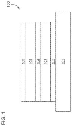
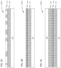
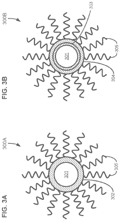
QNED displays utilize advanced quantum dot structures and compositions to enhance display quality. These structures often involve specific materials and arrangements to optimize light emission and color purity. Innovations in quantum dot design, such as core-shell structures or specific elemental compositions, contribute to improved display performance.- Quantum dot structure and composition: QNED displays utilize advanced quantum dot structures and compositions to enhance display quality. These structures often involve specific arrangements of nanoparticles or quantum wells that optimize light emission and color purity. The composition of these quantum dots, including core-shell structures and doping materials, plays a crucial role in determining the overall display performance.
- Light-emitting layer design: The design of the light-emitting layer is critical for QNED display quality. This includes the arrangement of quantum dots, the use of multiple emission layers, and the incorporation of charge transport materials. Optimizing the light-emitting layer structure can lead to improved brightness, color gamut, and energy efficiency in QNED displays.
- Color conversion and enhancement techniques: QNED displays employ various color conversion and enhancement techniques to achieve superior image quality. These may include the use of color filters, phosphors, or specialized quantum dot materials that can convert light to specific wavelengths. Advanced color management algorithms and hardware implementations are also utilized to optimize color reproduction and accuracy.
- Electrode and backplane technology: The quality of QNED displays is significantly influenced by the electrode and backplane technology used. This includes innovations in transparent conductive electrodes, thin-film transistor (TFT) designs, and driving circuits. Advanced electrode materials and structures can improve current distribution, reduce power consumption, and enhance overall display performance.
- Encapsulation and stability improvements: Ensuring the long-term stability and reliability of QNED displays is crucial for maintaining display quality over time. This involves developing advanced encapsulation techniques to protect quantum dots from environmental factors, as well as improving the overall device structure to enhance thermal stability and reduce degradation. These improvements contribute to longer display lifetimes and consistent performance.
02 Light-emitting layer configuration
The configuration of the light-emitting layer in QNED displays plays a crucial role in display quality. This includes the arrangement of quantum dots, the use of multiple layers, and the incorporation of other materials to enhance light emission and color reproduction. Optimizing the light-emitting layer structure can lead to improved brightness, contrast, and color gamut.Expand Specific Solutions03 Electrode and current injection optimization
Enhancing the electrode design and current injection methods in QNED displays can significantly impact display quality. This involves developing novel electrode materials, structures, and configurations to improve charge carrier injection and transport. Optimized current injection leads to more efficient light emission and better overall display performance.Expand Specific Solutions04 Color conversion and filtering techniques
QNED display quality can be enhanced through advanced color conversion and filtering techniques. This includes the use of specialized color filters, phosphors, or other materials to refine the spectral output of the quantum dots. These techniques help achieve more accurate color reproduction and a wider color gamut.Expand Specific Solutions05 Display panel structure and integration
The overall structure and integration of QNED display panels contribute to display quality. This involves optimizing the arrangement of various components, including the quantum dot layer, electrodes, and other functional layers. Innovations in panel design can lead to improved uniformity, reduced power consumption, and enhanced durability of QNED displays.Expand Specific Solutions
QNED Industry Leaders
The QNED (Quantum Nano Emitting Diode) display technology market is in its early growth stage, with significant potential for expansion. The global display market, valued at over $150 billion, presents a substantial opportunity for QNED adoption. While the technology is still emerging, major players like Samsung Display, LG Display, and BOE Technology Group are investing heavily in research and development. These companies, along with others like TCL China Star Optoelectronics and Sharp, are driving technological advancements. The maturity of QNED technology is progressing rapidly, with prototypes and early commercial products being showcased. However, mass production and widespread market penetration are still in development, indicating a competitive landscape poised for significant growth and innovation in the coming years.
BOE Technology Group Co., Ltd.
Technical Solution: BOE has developed QNED (Quantum Nano Emitting Diode) technology, which combines quantum dot and mini-LED technologies. Their QNED displays use a mini-LED backlight with quantum dot color conversion film to achieve high brightness, wide color gamut, and improved contrast. BOE's QNED panels feature over 10,000 local dimming zones, enabling precise control of brightness and contrast. The company has also integrated AI-powered image processing algorithms to enhance picture quality and optimize energy efficiency in real-time.
Strengths: Superior color performance, high brightness, and improved contrast compared to traditional LCD. Energy-efficient design. Weaknesses: Higher production costs than conventional LCDs, potential for blooming effects in high-contrast scenes.
Samsung Display Co., Ltd.
Technical Solution: Samsung has been developing its own version of QNED technology, which they call QD-OLED (Quantum Dot OLED). This hybrid display technology combines the benefits of QLED and OLED. Samsung's approach uses blue OLED material as the light source and quantum dots for color conversion. The company has invested heavily in research and development to overcome challenges such as blue OLED degradation and quantum dot efficiency. Samsung's QD-OLED displays offer perfect blacks, wide viewing angles, and a broader color gamut compared to traditional OLED panels.
Strengths: Excellent color reproduction, perfect blacks, and wide viewing angles. Potentially longer lifespan than traditional OLED. Weaknesses: Higher production costs, potential for burn-in (though reduced compared to standard OLED).
QNED Core Innovations
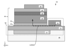
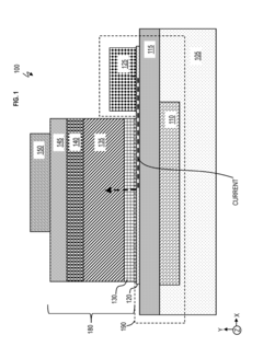
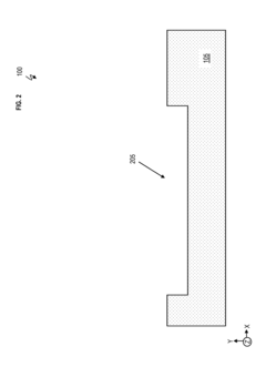
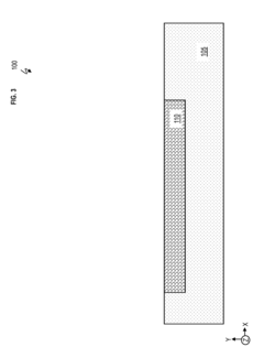
Vertically integrated nanotube and quantum dot LED for active matrix display
PatentActiveUS20180205031A1
Innovation
- A vertically integrated device structure using a semiconducting nanotube thin film as the anode for QDLEDs, where the nanotube film is transparent and its conductivity is tuned by an embedded local gate to control the drive current, allowing for effective pixel control and integration into an active matrix display.
Light-emitting apparatus with improved charge transport layer
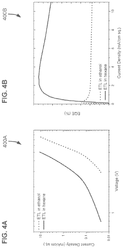
PatentPendingUS20240138178A1
Innovation
- Incorporating a metal-oxide nanoparticle-based electron transport layer with specific solvent polarity and size characteristics, which improves charge balance and injection efficiency by depositing nanoparticles in a multi-layer structure with varying sizes and polarities, potentially matching or exceeding the size of quantum dots.
QNED Manufacturing Process
The QNED (Quantum Nano Emitting Diode) manufacturing process represents a significant advancement in display technology, combining the benefits of quantum dots and mini-LED backlighting. This process involves several intricate steps to create a high-performance display panel.
The first stage of QNED manufacturing focuses on the production of quantum dots. These nanocrystals are synthesized using precise chemical processes, typically involving the combination of semiconductor materials such as cadmium selenide or indium phosphide. The size and composition of these quantum dots are carefully controlled to achieve specific color emission properties.
Once the quantum dots are produced, they are integrated into a film or layer that will be incorporated into the display panel. This integration process requires meticulous handling to ensure uniform distribution and prevent aggregation of the quantum dots, which could affect color accuracy and brightness.
The next critical step in QNED manufacturing is the production and placement of mini-LEDs. These tiny light-emitting diodes are fabricated using advanced semiconductor manufacturing techniques, often involving epitaxial growth processes. The mini-LEDs are then precisely positioned on a substrate, forming the backlight unit of the display.
The assembly of the QNED panel involves layering the quantum dot film over the mini-LED backlight unit. This step requires precise alignment and bonding techniques to ensure optimal light transmission and color conversion. Additional layers, such as diffusers and polarizers, are also incorporated to enhance the display's performance.
Quality control is a crucial aspect of the QNED manufacturing process. Each panel undergoes rigorous testing for color accuracy, brightness uniformity, and overall performance. Advanced imaging systems and spectrophotometers are employed to detect any defects or inconsistencies in the display output.
The final stages of QNED manufacturing involve the integration of the display panel with driving electronics and control systems. This includes the attachment of flexible printed circuits and the installation of timing controllers and power management units. The completed QNED module is then subjected to further testing and calibration before being integrated into the final product.
Throughout the manufacturing process, maintaining a clean and controlled environment is paramount. Many steps are carried out in cleanroom facilities to prevent contamination that could compromise the performance or longevity of the display. Additionally, the entire process requires sophisticated automation and precision robotics to achieve the necessary accuracy and consistency in production.
QNED Energy Efficiency
QNED (Quantum Nano Emitting Diode) technology represents a significant advancement in display energy efficiency, addressing one of the most critical challenges in modern display technologies. This innovative approach combines the benefits of quantum dots and mini-LED backlighting to achieve superior energy performance compared to traditional LCD and OLED displays.
At the core of QNED's energy efficiency is its unique light emission mechanism. By utilizing quantum dots, QNED displays can produce highly precise and saturated colors with minimal energy loss. This is achieved through the quantum confinement effect, where the size of the quantum dots determines the wavelength of emitted light. As a result, QNED displays can generate a wide color gamut while consuming less power than conventional display technologies.
The integration of mini-LED backlighting further enhances QNED's energy efficiency. Mini-LEDs allow for more precise local dimming, enabling the display to selectively illuminate only the necessary areas of the screen. This targeted approach significantly reduces power consumption, especially when displaying content with dark or black areas. The combination of quantum dots and mini-LEDs also improves light utilization, as the quantum dots can efficiently convert the blue light from the mini-LEDs into red and green light, minimizing energy waste in color conversion processes.
QNED displays also benefit from improved thermal management. The use of inorganic materials in quantum dots and mini-LEDs results in better heat dissipation compared to organic materials used in OLED displays. This enhanced thermal efficiency not only contributes to longer display lifespans but also reduces the energy required for cooling systems in devices, further improving overall energy efficiency.
Moreover, QNED technology offers superior brightness capabilities while maintaining energy efficiency. The high luminance output of mini-LEDs, combined with the color-enhancing properties of quantum dots, allows QNED displays to achieve higher peak brightness levels without a proportional increase in power consumption. This is particularly advantageous for HDR content and outdoor visibility, where high brightness is crucial.
The energy efficiency of QNED technology also extends to its manufacturing process. The production of QNED displays typically requires less energy-intensive processes compared to OLED manufacturing, potentially reducing the overall carbon footprint of display production. This aspect of energy efficiency is increasingly important as sustainability becomes a key consideration in technology development and consumer choices.
Unlock deeper insights with PatSnap Eureka Quick Research — get a full tech report to explore trends and direct your research. Try now!
Generate Your Research Report Instantly with AI Agent
Supercharge your innovation with PatSnap Eureka AI Agent Platform!