

How to Guide Display Transitions with QNED Implementation?
JUN 18, 20259 MIN READ
Generate Your Research Report Instantly with AI Agent
Patsnap Eureka helps you evaluate technical feasibility & market potential.
QNED Display Evolution
QNED (Quantum Nano Emitting Diode) display technology has undergone significant evolution since its inception, marking a new era in display innovation. This evolution has been driven by the quest for superior image quality, energy efficiency, and enhanced user experience in display technologies.
The journey of QNED displays began with the fundamental research into quantum dot technology, which forms the basis of QNED. Quantum dots, nanoscale semiconductor particles, were first discovered in the 1980s, but their application in displays only gained traction in the early 2000s. The initial focus was on improving color gamut and brightness in LCD displays by using quantum dots as a color conversion layer.
As research progressed, scientists and engineers recognized the potential of quantum dots as direct light emitters, leading to the concept of QNED. This marked a significant shift from using quantum dots merely as color enhancers to employing them as the primary light source in displays. The transition from concept to practical implementation involved overcoming numerous technical challenges, including improving quantum dot stability, enhancing electron injection efficiency, and developing suitable manufacturing processes.
The evolution of QNED displays has been characterized by several key milestones. Early prototypes demonstrated the feasibility of quantum dot-based light emission but struggled with issues such as low efficiency and short lifespans. Subsequent iterations focused on improving these aspects, with researchers exploring various quantum dot materials and structures to optimize performance.
A crucial breakthrough came with the development of cadmium-free quantum dots, addressing environmental concerns and paving the way for wider adoption. This was followed by advancements in quantum dot synthesis techniques, enabling better control over size distribution and, consequently, more precise color output.
The integration of QNED technology with existing display architectures has been another significant aspect of its evolution. Initially, QNED elements were incorporated into traditional LCD structures, creating hybrid displays that leveraged the strengths of both technologies. This approach allowed for a gradual transition, enabling manufacturers to adopt QNED technology without completely overhauling their production lines.
Recent developments in QNED evolution have focused on scaling up the technology for mass production. This has involved innovations in manufacturing processes, such as improved deposition techniques for quantum dot layers and the development of more efficient electron transport layers. Additionally, efforts have been made to enhance the longevity and stability of QNED displays, addressing concerns about degradation over time.
The evolution of QNED displays has also been influenced by parallel advancements in related technologies, such as micro-LED and OLED. This has led to a competitive landscape where QNED must continually innovate to maintain its position as a promising next-generation display technology.
Market Demand Analysis
The market demand for QNED (Quantum Nano-Emitting Diode) display technology is rapidly growing, driven by the increasing consumer appetite for high-quality visual experiences across various devices. As consumers seek more immersive and lifelike display solutions, QNED technology has emerged as a promising contender in the premium display market.
The global display market is projected to expand significantly in the coming years, with QNED technology poised to capture a substantial share. This growth is fueled by the rising adoption of advanced display technologies in smartphones, televisions, and other consumer electronics. QNED displays offer several advantages over existing technologies, including superior color accuracy, higher brightness, and improved energy efficiency, making them particularly attractive to consumers and manufacturers alike.
In the television segment, there is a strong demand for larger screen sizes with enhanced picture quality. QNED technology addresses this need by providing exceptional contrast ratios and wider color gamuts, rivaling OLED displays while potentially offering better longevity and reduced risk of burn-in. This positions QNED as a compelling option for high-end televisions and home theater systems.
The smartphone and tablet market also presents significant opportunities for QNED implementation. As mobile devices continue to serve as primary content consumption platforms, there is an increasing demand for displays that can deliver vibrant colors and high contrast ratios while maintaining energy efficiency. QNED technology's ability to meet these requirements makes it an attractive option for premium mobile devices.
Furthermore, the automotive industry is showing growing interest in advanced display technologies for in-vehicle infotainment systems and digital dashboards. QNED displays could offer improved visibility in varying light conditions and enhanced durability, addressing key concerns in automotive applications.
The professional display market, including monitors for content creation, graphic design, and medical imaging, is another area where QNED technology could see substantial demand. The technology's ability to provide accurate color reproduction and high contrast is particularly valuable in these specialized fields.
As the display industry continues to evolve, there is an increasing focus on sustainability and energy efficiency. QNED technology's potential for reduced power consumption compared to some existing display technologies aligns well with this trend, potentially driving further market demand.
In conclusion, the market demand for QNED display technology is robust and diverse, spanning multiple sectors including consumer electronics, automotive, and professional applications. The technology's ability to offer superior visual performance while addressing energy efficiency concerns positions it favorably in the competitive display market landscape.
QNED Tech Challenges
QNED (Quantum Nano Emitting Diode) technology faces several significant challenges in its implementation for display transitions. One of the primary hurdles is achieving consistent and uniform quantum dot emission across the entire display panel. The nano-scale nature of quantum dots makes it difficult to ensure even distribution and precise control over their placement, leading to potential color inconsistencies and brightness variations during transitions.
Another major challenge lies in the stability and longevity of quantum dots. These nanoparticles are susceptible to degradation over time, especially when exposed to heat and light. This degradation can result in color shifts and reduced brightness, affecting the overall quality of display transitions. Developing robust encapsulation methods to protect quantum dots from environmental factors is crucial for maintaining consistent performance throughout the device's lifespan.
The integration of QNED technology with existing display architectures presents additional complexities. Adapting current manufacturing processes to incorporate quantum dot layers without compromising other display components requires significant engineering efforts. Moreover, ensuring compatibility with various backlight technologies and color filter designs adds another layer of complexity to the implementation process.
Color accuracy and gamut expansion are key objectives in QNED development, but they also pose technical challenges. Achieving precise color control during transitions demands sophisticated algorithms and hardware capable of rapidly adjusting quantum dot emission characteristics. Expanding the color gamut while maintaining energy efficiency is a delicate balance that requires ongoing research and innovation in materials science and optical engineering.
The scalability of QNED technology for different display sizes and resolutions is another area of concern. As display resolutions continue to increase, the density of quantum dots must be adjusted accordingly without sacrificing uniformity or performance. This scaling challenge becomes particularly evident when transitioning between different content types or display modes, where the quantum dot response must be consistently rapid and accurate across varying pixel densities.
Heat management is a critical issue in QNED displays, especially during high-brightness transitions. Quantum dots can be sensitive to temperature fluctuations, which can affect their emission properties. Developing effective thermal management solutions that can rapidly dissipate heat without adding significant bulk or cost to the display is essential for maintaining stable performance during dynamic transitions.
Lastly, the cost-effectiveness of QNED technology remains a challenge for widespread adoption. The production of high-quality quantum dots and their integration into display panels is currently more expensive than traditional display technologies. Reducing manufacturing costs while maintaining performance standards is crucial for QNED to compete in the consumer electronics market and enable smooth, high-quality display transitions across a range of devices.
Current QNED Solutions
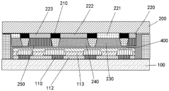
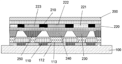
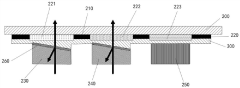
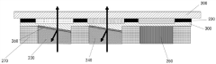
01 QNED structure and composition
QNED displays utilize quantum nano-emitting diodes, which are composed of quantum dots and nanoparticles. These structures are designed to enhance light emission efficiency and color purity. The quantum dots are typically made of semiconductor materials and are engineered to specific sizes to control the wavelength of emitted light.- Quantum dot-based light emitting diode structure: QNED displays utilize quantum dot-based light emitting diodes (QD-LEDs) as the core component. These structures typically consist of a quantum dot emissive layer sandwiched between electron and hole transport layers. The quantum dots are engineered to emit specific colors when electrically excited, providing high color purity and efficiency for display applications.
- Nanorod-based QNED devices: Some QNED designs incorporate nanorods instead of or in addition to quantum dots. These nanorod structures can offer advantages in terms of light emission directionality and efficiency. The nanorods are typically arranged in a specific orientation within the device to optimize performance.
- Manufacturing processes for QNED displays: Various manufacturing techniques are employed to produce QNED displays, including solution processing methods, vapor deposition, and transfer printing. These processes focus on precisely depositing and patterning the quantum dot or nanorod layers, as well as the surrounding transport and electrode layers, to create high-performance devices at scale.
- Color conversion and enhancement in QNED displays: QNED technology often incorporates color conversion or enhancement layers to improve display performance. This can involve using quantum dots or other nanostructures to convert blue or UV light from a backlight into precise red and green wavelengths, resulting in improved color gamut and efficiency compared to traditional LCD displays.
- Integration with other display technologies: QNED technology is being integrated with other display technologies to create hybrid solutions. This includes combining QNED elements with OLED or mini-LED backlight systems to leverage the strengths of multiple approaches. These hybrid designs aim to achieve optimal performance in terms of color quality, contrast, and energy efficiency.
02 Fabrication methods for QNED displays
Various fabrication techniques are employed in the production of QNED displays, including solution processing, vapor deposition, and patterning methods. These processes aim to create uniform and precise quantum dot layers, ensuring optimal performance of the display. Advanced manufacturing techniques are developed to improve yield and reduce production costs.Expand Specific Solutions03 Color conversion and light management
QNED displays often incorporate color conversion layers and light management techniques to enhance display performance. This includes the use of color filters, reflective layers, and optical structures to improve color gamut, contrast, and energy efficiency. Advanced designs focus on optimizing light extraction and reducing optical losses within the display stack.Expand Specific Solutions04 Integration with existing display technologies
QNED technology is being integrated with existing display technologies such as LCD and OLED to create hybrid solutions. These combinations aim to leverage the strengths of multiple technologies, potentially offering improved performance in areas like brightness, color accuracy, and power efficiency. Transition strategies are developed to incorporate QNED elements into established manufacturing processes.Expand Specific Solutions05 Addressing challenges in QNED technology
Ongoing research focuses on overcoming challenges in QNED technology, including improving stability, longevity, and uniformity of quantum dot emitters. Efforts are made to enhance electron injection and transport within the device structure, reduce degradation mechanisms, and develop encapsulation techniques to protect sensitive materials from environmental factors.Expand Specific Solutions
Key QNED Players
The QNED (Quantum Nano Emitting Diode) display technology market is in its early growth stage, with significant potential for expansion. The global QNED market size is projected to grow rapidly, driven by increasing demand for high-quality displays in various sectors. Technologically, QNED is still evolving, with companies like BOE Technology Group, LG Display, and Samsung Display leading the development. These firms are investing heavily in R&D to enhance QNED's performance and cost-effectiveness. Other players like Sharp, TCL, and Huawei are also making strides in this field, contributing to the technology's maturation. The competitive landscape is characterized by intense innovation and strategic partnerships, as companies aim to establish dominance in this promising display technology sector.
BOE Technology Group Co., Ltd.
Technical Solution: BOE has developed a QNED (Quantum Nano Emitting Diode) display technology that combines quantum dot and mini-LED technologies. Their implementation focuses on enhancing color gamut, contrast ratio, and brightness while reducing power consumption. BOE's QNED displays use a blue mini-LED backlight combined with red and green quantum dots, allowing for precise local dimming and improved HDR performance. The company has also developed advanced driving algorithms to optimize the transition between different brightness levels and color states, ensuring smooth and natural display transitions.
Strengths: Wide color gamut, high contrast ratio, and energy efficiency. Weaknesses: Higher production costs compared to traditional LCD, and potential for image retention in static content scenarios.
LG Display Co., Ltd.
Technical Solution: LG Display has introduced QNED technology in their TV lineup, utilizing mini-LED backlighting combined with quantum dot technology. Their implementation focuses on creating smoother transitions between scenes with varying brightness and color intensity. LG's QNED displays employ a sophisticated local dimming algorithm that adjusts the mini-LED backlight in real-time, reducing blooming effects and enhancing contrast. To guide display transitions, LG has developed an AI-powered processor that analyzes content frame by frame, predicting and optimizing the backlight and quantum dot layer's response for seamless scene changes.
Strengths: Advanced AI-driven transition optimization, reduced blooming effect. Weaknesses: Higher cost compared to conventional LED-LCD TVs, potential for slight color shift at extreme viewing angles.
QNED Core Innovations
Display panel
PatentPendingCN114914271A
Innovation
- By arranging a wavelength conversion unit and a color filter unit located on the light exit side of the wavelength conversion unit in the display panel, the optical path of the unconverted blue light in the color conversion unit is extended, and the pattern and tilt angle of the color filter unit are used to improve the light conversion efficiency.
Quantum-nano light emitting diode pixel and quantum-nano light emitting diode display device
PatentActiveKR1020190029831A
Innovation
- Incorporating a switching transistor, storage capacitor, driving transistor, and sensing transistors to sense and compensate for ohmic contact resistance variations, using inorganic materials like gallium nitride for Q-NEDs, and employing a sensing operation to adjust data voltages based on sensed resistances.


QNED Manufacturing
The manufacturing process of QNED (Quantum Nano Emitting Diode) displays involves several complex steps that require precision engineering and advanced technologies. The production begins with the preparation of the quantum dot material, which is typically composed of semiconductor nanocrystals. These quantum dots are synthesized using colloidal chemistry techniques, allowing for precise control over their size and composition.
Once the quantum dots are prepared, they are integrated into a thin-film structure that forms the emissive layer of the display. This integration process often involves techniques such as spin-coating or inkjet printing, which allow for uniform deposition of the quantum dot material across the substrate. The substrate itself is usually made of glass or a flexible material, depending on the desired characteristics of the final display.
The next critical step in QNED manufacturing is the creation of the micro-LED array. This process involves the fabrication of miniature LED chips, typically using gallium nitride (GaN) or indium gallium nitride (InGaN) semiconductors. These micro-LEDs are produced using advanced lithography and etching techniques to achieve the necessary small size and high density required for high-resolution displays.
Following the production of the micro-LED array, the quantum dot layer is carefully aligned and bonded to the LED structure. This alignment process is crucial for ensuring that each quantum dot corresponds precisely to its respective micro-LED, enabling accurate color reproduction and high efficiency. Advanced pick-and-place technologies or transfer printing methods are often employed to achieve this precise alignment.
The manufacturing process also includes the integration of the backplane electronics, which control the individual pixels of the display. This typically involves the fabrication of thin-film transistors (TFTs) on the substrate, which are responsible for addressing and driving each pixel. The TFT backplane is usually produced using low-temperature polycrystalline silicon (LTPS) or oxide semiconductor technologies.
To protect the delicate quantum dot and micro-LED structures, encapsulation layers are applied. These layers serve to prevent moisture and oxygen ingress, which can degrade the performance and lifespan of the display. Advanced barrier films and sealing technologies are employed to ensure long-term stability and reliability of the QNED display.
Finally, the manufacturing process concludes with the integration of additional optical components, such as color filters and polarizers, which further enhance the display's visual performance. Quality control measures, including optical and electrical testing, are implemented throughout the production process to ensure that each QNED display meets the required specifications for brightness, color accuracy, and uniformity.
QNED Energy Efficiency
QNED (Quantum Nano Emitting Diode) technology has shown promising potential in improving energy efficiency for display applications. The implementation of QNED in display transitions offers significant advantages in terms of power consumption and overall energy efficiency.
QNED displays utilize quantum dots and nanorod LEDs to produce highly efficient and vibrant colors. This technology allows for precise control over light emission, resulting in reduced energy waste compared to traditional display technologies. The nano-scale size of the quantum dots enables more efficient conversion of electrical energy into light, minimizing heat generation and power loss.
One of the key factors contributing to QNED's energy efficiency is its ability to achieve high brightness levels with lower power input. This is particularly beneficial during display transitions, where rapid changes in brightness and color are required. The quick response time of QNED pixels allows for smoother transitions without the need for excessive power consumption.
Furthermore, QNED technology enables local dimming with greater precision than conventional LED-backlit displays. This feature allows for selective illumination of specific areas of the screen, reducing power consumption in darker regions while maintaining high contrast and image quality. During display transitions, this localized control can be leveraged to optimize energy usage by selectively activating only the necessary pixels.
The color gamut capabilities of QNED displays also contribute to energy efficiency. With a wider color range and more accurate color reproduction, QNED panels can achieve the desired visual output with less power input. This is particularly advantageous during color-intensive transitions, where traditional displays might require more energy to produce vibrant and accurate colors.
QNED's energy efficiency extends to its thermal management properties. The reduced heat generation compared to conventional display technologies translates to lower cooling requirements, further reducing overall power consumption. This aspect is crucial for maintaining consistent performance during prolonged use and frequent display transitions.
In the context of display transitions, QNED's energy efficiency also manifests in its ability to maintain image quality at lower refresh rates. This allows for smoother transitions without the need for high-frequency updates, which can be power-intensive in other display technologies.
As QNED technology continues to evolve, further improvements in energy efficiency are expected. Ongoing research focuses on enhancing quantum dot efficiency, optimizing nanorod LED structures, and developing advanced control algorithms for display transitions. These advancements promise to push the boundaries of energy-efficient display technology, making QNED an increasingly attractive option for next-generation displays across various applications.
Unlock deeper insights with Patsnap Eureka Quick Research — get a full tech report to explore trends and direct your research. Try now!
Generate Your Research Report Instantly with AI Agent
Supercharge your innovation with Patsnap Eureka AI Agent Platform!