Exploring cross-disciplinary innovations driven by silicon photonics.
JUL 17, 20259 MIN READ
Generate Your Research Report Instantly with AI Agent
PatSnap Eureka helps you evaluate technical feasibility & market potential.
Silicon Photonics Evolution
Silicon photonics has undergone a remarkable evolution since its inception in the late 1980s. The field emerged from the convergence of optical communication technologies and semiconductor manufacturing processes, driven by the need for high-speed, low-power data transmission in computing and telecommunications.
In the early stages, researchers focused on developing basic building blocks such as waveguides, modulators, and detectors on silicon substrates. The 1990s saw significant advancements in fabrication techniques, enabling the creation of more complex photonic structures. This period also witnessed the development of silicon-based light sources, a crucial component for fully integrated photonic circuits.
The turn of the millennium marked a pivotal moment in silicon photonics evolution. The introduction of silicon-on-insulator (SOI) technology provided a platform for low-loss waveguides and enhanced light confinement. This breakthrough accelerated the development of integrated photonic devices and circuits, paving the way for practical applications in data centers and telecommunications networks.
From 2005 to 2015, silicon photonics experienced rapid growth and commercialization. Major tech companies and startups invested heavily in the technology, recognizing its potential to address the bandwidth and energy efficiency challenges in data centers. This period saw the emergence of the first commercial silicon photonics transceivers and the integration of photonic components with electronic circuits.
Recent years have witnessed a shift towards exploring cross-disciplinary applications of silicon photonics. The technology has found its way into diverse fields such as biosensing, quantum computing, and artificial intelligence. Researchers are now investigating novel materials and hybrid integration techniques to overcome the limitations of pure silicon-based devices and expand the functionality of photonic circuits.
The evolution of silicon photonics has been characterized by continuous improvements in performance, integration density, and cost-effectiveness. From initial proof-of-concept demonstrations to today's commercial products, the field has made significant strides in bridging the gap between electronics and photonics. As we look to the future, silicon photonics is poised to play a crucial role in enabling next-generation technologies across multiple industries, driving innovation and shaping the landscape of cross-disciplinary research and development.
Market Demand Analysis
Silicon photonics has emerged as a transformative technology, driving significant market demand across various industries. The integration of optical and electronic components on a single chip has opened up new possibilities for high-speed data transmission, sensing, and computing applications. The global silicon photonics market is experiencing rapid growth, with projections indicating a compound annual growth rate (CAGR) of over 20% in the coming years.
One of the primary drivers of market demand for silicon photonics is the telecommunications sector. As data traffic continues to surge, telecom companies are seeking solutions to enhance network capacity and reduce power consumption. Silicon photonics offers a promising avenue for addressing these challenges, enabling faster data transmission rates and improved energy efficiency in optical communication systems.
The data center industry represents another significant market for silicon photonics innovations. With the exponential growth of cloud computing and big data analytics, data centers require increasingly higher bandwidth and lower latency interconnects. Silicon photonics-based transceivers and interconnects are gaining traction in this sector, offering superior performance and scalability compared to traditional copper-based solutions.
In the healthcare and life sciences domain, silicon photonics is driving advancements in biosensing and diagnostic technologies. The ability to integrate multiple optical functions on a single chip enables the development of compact, highly sensitive biosensors for applications such as point-of-care diagnostics and environmental monitoring. This has led to increased demand from both research institutions and medical device manufacturers.
The automotive industry is also showing growing interest in silicon photonics, particularly for LiDAR (Light Detection and Ranging) systems in autonomous vehicles. Silicon photonics-based LiDAR offers the potential for more compact, cost-effective, and high-performance sensing solutions, which are crucial for the widespread adoption of self-driving technologies.
Furthermore, the emerging field of quantum computing is creating new market opportunities for silicon photonics. Quantum photonic circuits based on silicon platforms are being explored for quantum information processing and communication, attracting investments from both established tech giants and startups.
As cross-disciplinary innovations continue to evolve, the market demand for silicon photonics is expected to expand into new application areas. These include augmented and virtual reality systems, aerospace and defense technologies, and next-generation artificial intelligence hardware. The versatility and scalability of silicon photonics make it an attractive technology for addressing diverse market needs across multiple industries.
Technical Challenges
Silicon photonics has emerged as a transformative technology, offering unprecedented opportunities for cross-disciplinary innovations. However, the field faces several significant technical challenges that must be addressed to fully realize its potential.
One of the primary challenges in silicon photonics is the integration of diverse optical components on a single chip. While silicon is an excellent material for waveguides and passive structures, it lacks efficient light emission and detection capabilities. This limitation necessitates the development of hybrid integration techniques to incorporate III-V materials or other active elements onto silicon platforms. The process of achieving seamless integration while maintaining high performance and reliability remains a complex task.
Another critical challenge lies in the realm of optical modulation and switching. As data rates continue to increase, there is a growing demand for faster and more efficient modulators. Current silicon-based modulators often struggle to meet the stringent requirements for high-speed operation and low power consumption. Researchers are exploring novel approaches, such as plasmonic modulators and electro-optic materials, to overcome these limitations and push the boundaries of modulation speeds.
Thermal management presents yet another hurdle in silicon photonics. The temperature sensitivity of optical components can lead to performance degradation and wavelength drift. Developing effective thermal control strategies and athermal designs is crucial for ensuring stable operation across a wide range of environmental conditions. This challenge becomes particularly acute in high-density photonic integrated circuits where heat dissipation is a significant concern.
The field also grapples with challenges related to packaging and testing of photonic integrated circuits. Unlike electronic integrated circuits, photonic devices require precise optical alignment and coupling, which can be difficult to achieve at scale. Developing standardized packaging solutions and automated testing methodologies is essential for enabling cost-effective mass production of silicon photonic devices.
Furthermore, the miniaturization of photonic components poses unique challenges. As devices shrink to nanoscale dimensions, phenomena such as surface roughness and quantum effects become increasingly significant. Overcoming these effects while maintaining high performance requires innovative design approaches and advanced fabrication techniques.
Lastly, the cross-disciplinary nature of silicon photonics itself presents a challenge in terms of knowledge integration and collaboration. Bridging the gap between optics, electronics, materials science, and other related fields requires a concerted effort to foster interdisciplinary research and development. This challenge extends beyond technical aspects to include education, training, and the establishment of common standards and practices across different domains.
Current Solutions
01 Optical interconnects and communication systems
Silicon photonics technology is utilized in developing high-speed optical interconnects and communication systems. These systems integrate optical components on silicon chips to enable efficient data transmission and processing in various applications, including data centers and telecommunications networks.- Optical interconnects and data transmission: Silicon photonics technology is utilized for high-speed optical interconnects and data transmission in computing and communication systems. This includes the development of integrated photonic circuits that can transmit and process optical signals efficiently, enabling faster data transfer rates and reduced power consumption compared to traditional electronic interconnects.
- Integration of photonic and electronic components: Silicon photonics enables the integration of photonic and electronic components on a single chip or package. This integration allows for the creation of compact, high-performance devices that combine the advantages of both optical and electronic technologies, leading to improved functionality and reduced form factors in various applications.
- Waveguide structures and optical modulators: Advanced waveguide structures and optical modulators are key components in silicon photonics. These elements are designed to guide and manipulate light signals efficiently within integrated photonic circuits, enabling precise control over optical properties such as phase, amplitude, and polarization for various applications in optical communication and sensing.
- Photonic sensors and detectors: Silicon photonics technology is applied in the development of highly sensitive photonic sensors and detectors. These devices leverage the unique properties of silicon-based photonic structures to achieve improved performance in applications such as environmental monitoring, biomedical sensing, and optical signal detection for communication systems.
- Quantum photonics and emerging applications: Silicon photonics is being explored for quantum photonics applications and other emerging fields. This includes the development of quantum light sources, quantum memories, and integrated quantum circuits that can leverage the scalability and compatibility of silicon-based fabrication processes for potential breakthroughs in quantum computing and communication.
02 Integration of photonic and electronic components
Silicon photonics allows for the integration of photonic and electronic components on a single chip. This integration enables the development of compact, energy-efficient devices that combine the advantages of both optical and electronic technologies for improved performance in computing and communication applications.Expand Specific Solutions03 Waveguide structures and optical modulators
Advanced waveguide structures and optical modulators are key components in silicon photonics. These elements are designed to efficiently guide and manipulate light on silicon chips, enabling high-speed data transmission and processing in photonic integrated circuits.Expand Specific Solutions04 Photonic sensors and detectors
Silicon photonics technology is applied in the development of highly sensitive photonic sensors and detectors. These devices utilize the interaction between light and silicon structures to detect various physical, chemical, or biological parameters, offering potential applications in environmental monitoring, healthcare, and industrial sensing.Expand Specific Solutions05 Quantum photonics and integrated lasers
Silicon photonics is advancing in the field of quantum photonics and integrated lasers. Researchers are exploring ways to incorporate quantum light sources and detectors on silicon chips, as well as developing efficient on-chip lasers to enable fully integrated photonic systems for quantum computing and communication applications.Expand Specific Solutions
Key Industry Players
The silicon photonics market is experiencing rapid growth and cross-disciplinary innovation, driven by increasing demand for high-speed data transmission and integrated photonic circuits. The industry is in a transitional phase, moving from early adoption to mainstream implementation across various sectors. Market size is projected to expand significantly, with key players like Intel, IBM, and Huawei investing heavily in research and development. Technological maturity varies, with companies like GlobalFoundries and TSMC leading in manufacturing processes, while academic institutions such as MIT and Zhejiang University contribute to fundamental research. Emerging players like Skorpios Technologies and Advanced Micro Foundry are pushing boundaries in specialized applications, indicating a dynamic and competitive landscape.
Huawei Technologies Co., Ltd.
Technical Solution: Huawei has made significant strides in silicon photonics, developing a 400G optical module based on silicon photonics technology[1]. Their approach integrates multiple optical functions onto a single chip, including modulators, photodetectors, and multiplexers. This integration allows for higher data transmission rates while reducing power consumption and form factor. Huawei's silicon photonics technology also incorporates advanced packaging techniques, enabling better thermal management and improved signal integrity[2]. The company has demonstrated the ability to scale this technology to support future 800G and 1.6T optical transceivers, positioning them at the forefront of high-speed optical communications[3].
Strengths: Advanced integration capabilities, high-speed data transmission, and scalability for future needs. Weaknesses: Potential dependence on external foundries for chip fabrication and challenges in achieving cost-effectiveness at scale.
International Business Machines Corp.
Technical Solution: IBM has been a pioneer in silicon photonics, developing a fully integrated wavelength multiplexed silicon photonics chip[4]. Their technology combines multiple optical components, including modulators, wavelength multiplexers, and photodetectors, on a single chip manufactured using standard CMOS processes. IBM's approach enables data transfer rates of up to 100 Gb/s per wavelength, with the potential for terabit-scale optical links[5]. The company has also demonstrated novel concepts such as optical switching matrices and on-chip optical frequency combs, pushing the boundaries of silicon photonics applications beyond traditional communications[6]. IBM's research extends to neuromorphic computing, where they explore the use of silicon photonics for implementing artificial neural networks with unprecedented speed and energy efficiency[7].
Strengths: Long-standing expertise in silicon photonics, integration with CMOS processes, and diverse application exploration. Weaknesses: Challenges in transitioning from research to large-scale commercial production and potential competition from specialized photonics companies.
Core Innovations
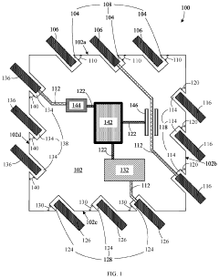
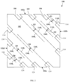
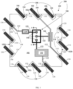
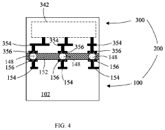
Photonics chips and semiconductor products having angled optical fibers
PatentActiveUS20230127056A1
Innovation
- The development of PIC chips with substrates featuring grooves angled at 30 to 60 degrees, preferably 45 degrees, along the edges to accommodate optical fibers, allowing for increased edge utilization and efficient optical signal transmission by positioning fibers within these grooves, thereby enhancing data density and communication capabilities.
Integration Strategies
Silicon photonics integration strategies are crucial for realizing the full potential of cross-disciplinary innovations in this field. The integration of photonic components with electronic circuits on a single chip presents both challenges and opportunities. One key strategy involves the development of hybrid integration techniques that combine the strengths of different material platforms.
Monolithic integration, where both photonic and electronic components are fabricated on the same substrate, offers advantages in terms of compactness and reduced parasitic effects. However, it requires careful consideration of material compatibility and process optimization. Heterogeneous integration, on the other hand, allows for the combination of disparate materials and technologies, enabling the incorporation of high-performance III-V lasers and detectors with silicon photonic circuits.
3D integration strategies are gaining traction, leveraging advanced packaging techniques to stack multiple layers of photonic and electronic components. This approach not only increases functional density but also enables novel architectures for signal processing and data transmission. Wafer-level bonding and through-silicon vias (TSVs) are key enabling technologies for this integration strategy.
Photonic-electronic co-design is emerging as a critical strategy to optimize system performance. This approach considers the interplay between photonic and electronic components from the earliest stages of design, leading to more efficient and robust integrated systems. Advanced simulation tools and design automation software are being developed to support this holistic approach to integration.
Integration of novel materials, such as graphene and other 2D materials, with silicon photonics platforms is opening up new possibilities for enhanced functionality and performance. These materials offer unique optical and electronic properties that can complement traditional silicon-based devices, enabling new classes of integrated photonic systems.
Packaging and thermal management strategies are also evolving to address the specific needs of integrated photonic systems. Novel approaches to fiber coupling, hermetic sealing, and heat dissipation are being developed to ensure reliable operation of complex photonic-electronic integrated circuits in real-world applications.
As integration strategies continue to advance, standardization efforts are underway to establish common interfaces and protocols for photonic integrated circuits. This will facilitate the development of a robust ecosystem for silicon photonics, enabling easier integration of components from different suppliers and accelerating the adoption of this technology across various industries.
Ecosystem Development
The development of a robust ecosystem is crucial for the advancement and widespread adoption of silicon photonics-driven cross-disciplinary innovations. This ecosystem encompasses a diverse range of stakeholders, including academic institutions, research laboratories, semiconductor manufacturers, photonics companies, and end-users across various industries.
Academic institutions and research laboratories play a pivotal role in pushing the boundaries of silicon photonics technology. They contribute to fundamental research, exploring novel materials, device architectures, and integration techniques. Collaborations between universities and industry partners foster knowledge transfer and accelerate the transition from laboratory discoveries to practical applications.
Semiconductor manufacturers are essential in scaling up the production of silicon photonics components. Their expertise in high-volume manufacturing processes and quality control is vital for reducing costs and improving the reliability of photonic integrated circuits. As the demand for silicon photonics grows, these manufacturers are investing in specialized fabrication facilities and developing new manufacturing techniques tailored to photonic devices.
Photonics companies specializing in design, packaging, and testing of photonic integrated circuits form another critical part of the ecosystem. These firms bridge the gap between raw semiconductor capabilities and application-specific solutions, offering design services, software tools, and specialized packaging solutions to meet the diverse needs of different industries.
End-users across various sectors, including telecommunications, data centers, healthcare, and automotive, drive the demand for silicon photonics-based innovations. Their requirements shape the direction of research and development efforts, pushing for higher performance, lower power consumption, and increased functionality.
To foster ecosystem growth, industry consortia and standards organizations play a crucial role in establishing common platforms, interfaces, and protocols. These efforts promote interoperability and reduce barriers to entry for new players, accelerating innovation and market adoption.
Government agencies and funding bodies contribute to ecosystem development by providing financial support for research initiatives, start-ups, and collaborative projects. Their investments help de-risk early-stage technologies and support the transition from research to commercialization.
As the silicon photonics ecosystem matures, it is increasingly intersecting with other emerging technologies such as artificial intelligence, quantum computing, and 5G/6G communications. This convergence is creating new opportunities for cross-disciplinary innovations, further expanding the potential applications and impact of silicon photonics technology.
Unlock deeper insights with PatSnap Eureka Quick Research — get a full tech report to explore trends and direct your research. Try now!
Generate Your Research Report Instantly with AI Agent
Supercharge your innovation with PatSnap Eureka AI Agent Platform!