How silicon photonics bridges communication latency challenges.
JUL 17, 20259 MIN READ
Generate Your Research Report Instantly with AI Agent
Patsnap Eureka helps you evaluate technical feasibility & market potential.
Silicon Photonics Evolution
Silicon photonics has undergone a remarkable evolution since its inception in the late 1980s. The technology has progressed from initial conceptualization to practical implementation, driven by the increasing demand for high-speed data transmission and low-latency communication. The journey of silicon photonics can be traced through several key developmental stages, each marked by significant technological advancements and breakthroughs.
In the early 1990s, researchers began exploring the potential of integrating photonic components with silicon-based electronic circuits. This period saw the development of fundamental building blocks such as waveguides, modulators, and detectors on silicon substrates. However, these early devices faced challenges in terms of efficiency and integration density.
The turn of the millennium brought about a surge in research activities, focusing on improving the performance and scalability of silicon photonic devices. This era witnessed the emergence of high-quality silicon-on-insulator (SOI) wafers, which became the preferred platform for silicon photonics. The development of advanced fabrication techniques, such as deep-UV lithography, enabled the creation of more complex and precise photonic structures.
Between 2005 and 2010, silicon photonics saw significant advancements in key components. Researchers achieved breakthroughs in high-speed modulators, efficient photodetectors, and low-loss waveguides. This period also marked the beginning of efforts to integrate multiple photonic functions on a single chip, paving the way for more compact and cost-effective solutions.
The following years, from 2010 to 2015, were characterized by the transition from research prototypes to commercial products. Major semiconductor companies and startups began investing heavily in silicon photonics, recognizing its potential to address the growing bandwidth demands in data centers and telecommunications. This phase saw the introduction of the first commercial transceivers based on silicon photonics technology.
From 2015 onwards, silicon photonics entered a phase of rapid commercialization and diversification. The technology found applications beyond data communications, expanding into areas such as sensing, quantum computing, and artificial intelligence. Advancements in packaging and integration techniques allowed for the development of more sophisticated photonic integrated circuits (PICs) with enhanced functionality and performance.
Recent years have witnessed a focus on addressing the challenges of communication latency through silicon photonics. Researchers and industry players have been working on developing ultra-low latency interconnects, exploring novel architectures such as photonic neural networks, and pushing the boundaries of integration density. These efforts aim to leverage the inherent advantages of light-based communication to minimize signal propagation delays and processing times.
As we look to the future, silicon photonics continues to evolve, with ongoing research into new materials, structures, and integration schemes. The technology is poised to play a crucial role in addressing the latency challenges in next-generation computing and communication systems, promising to revolutionize data transfer speeds and energy efficiency across various applications.
Communication Latency Market
The communication latency market is experiencing significant growth and transformation driven by the increasing demand for low-latency solutions across various industries. As data-intensive applications and real-time services become more prevalent, the need for faster and more efficient communication networks has become paramount. This market encompasses a wide range of technologies and solutions aimed at reducing latency in data transmission and processing.
The financial sector, particularly high-frequency trading, has been a major driver of the low-latency market. Milliseconds can make a substantial difference in trading outcomes, leading to substantial investments in ultra-low-latency solutions. Similarly, the gaming industry has seen a surge in demand for low-latency networks to enhance online gaming experiences and support cloud gaming platforms.
Emerging technologies such as 5G, edge computing, and the Internet of Things (IoT) are also fueling the growth of the communication latency market. These technologies require minimal delay in data transmission to function effectively, creating new opportunities for low-latency solution providers. The automotive industry, with the development of autonomous vehicles and vehicle-to-everything (V2X) communication, is another sector driving demand for ultra-low-latency networks.
The market is characterized by a mix of established telecommunications companies, networking equipment manufacturers, and innovative startups focusing on specialized low-latency solutions. Competition is fierce, with companies constantly pushing the boundaries of what's possible in terms of reducing latency.
Geographically, North America and Asia-Pacific are the leading regions in the communication latency market, with Europe following closely. The concentration of financial centers, technology hubs, and early 5G adopters in these regions contributes to their market dominance.
Looking ahead, the communication latency market is poised for continued growth. The proliferation of artificial intelligence and machine learning applications, the expansion of edge computing, and the ongoing rollout of 5G networks are expected to drive further demand for low-latency solutions. Additionally, as more industries recognize the importance of real-time data processing and communication, the market is likely to expand into new sectors, creating diverse opportunities for innovation and growth.
Current Challenges in Latency
As communication networks continue to expand and evolve, latency has emerged as a critical challenge in modern data transmission systems. The increasing demand for high-speed, low-latency communication has pushed traditional electronic systems to their limits, creating a need for innovative solutions. Silicon photonics, a technology that integrates optical components with silicon-based electronics, has shown promise in addressing these latency challenges.
One of the primary challenges in current communication systems is the inherent delay caused by electronic signal processing. As data rates increase, the time required for electronic components to process and route signals becomes a significant bottleneck. This electronic bottleneck is particularly evident in data centers and high-performance computing environments, where microseconds of delay can have substantial impacts on overall system performance.
Another major challenge is the physical limitations of copper-based interconnects. As data rates increase, the signal integrity of electrical signals transmitted over copper wires degrades rapidly, necessitating complex signal conditioning and error correction techniques. These additional processing steps further contribute to latency, creating a compounding effect that limits the scalability of traditional electronic systems.
The growing complexity of network architectures also presents latency challenges. As networks become more distributed and interconnected, data must traverse multiple hops and network layers, each introducing additional delay. This is particularly problematic in edge computing and Internet of Things (IoT) applications, where real-time responsiveness is crucial.
Energy consumption is another significant concern related to latency. As data centers and communication networks strive to reduce latency, they often rely on increased processing power and more complex routing algorithms. This approach leads to higher energy consumption, which not only increases operational costs but also contributes to environmental concerns.
Lastly, the increasing adoption of cloud services and distributed computing models has heightened the importance of minimizing latency in wide-area networks (WANs). The geographical distance between data centers and end-users introduces propagation delays that cannot be easily mitigated through traditional means, creating a need for novel approaches to reduce end-to-end latency in long-distance communications.
These challenges collectively underscore the limitations of current electronic-based communication systems in meeting the growing demand for low-latency, high-bandwidth data transmission. As a result, there is a pressing need for innovative technologies that can overcome these limitations and pave the way for next-generation communication networks.
Existing Latency Solutions
01 Optical interconnects for low latency communication
Silicon photonics technology is used to develop optical interconnects that can significantly reduce latency in data transmission. These interconnects leverage the high-speed capabilities of light for signal propagation, enabling faster data transfer compared to traditional electronic interconnects. This approach is particularly beneficial in high-performance computing and data center applications where minimizing latency is crucial.- Optical interconnects for low latency communication: Silicon photonics technology is used to develop optical interconnects that can significantly reduce latency in data transmission. These interconnects leverage the high-speed capabilities of light for signal propagation, enabling faster data transfer compared to traditional electronic interconnects. This approach is particularly beneficial in high-performance computing and data center applications where minimizing latency is crucial.
- Integration of photonic and electronic components: Advanced integration techniques are employed to combine photonic and electronic components on a single chip or package. This integration allows for seamless conversion between optical and electrical signals, reducing the overall system latency. The close proximity of these components minimizes signal travel distances and enables more efficient data processing and transmission.
- Optimized photonic circuit design: Innovative photonic circuit designs are developed to minimize signal propagation delays within silicon photonic devices. These designs focus on optimizing waveguide structures, reducing bend losses, and implementing efficient routing strategies. By carefully engineering the photonic components, the overall latency of the system can be significantly reduced.
- High-speed modulators and detectors: Advanced modulators and detectors are crucial components in silicon photonics for achieving low latency. High-speed modulators enable rapid conversion of electrical signals to optical signals, while fast detectors allow for quick conversion of optical signals back to electrical signals. These components are designed to operate at very high frequencies, minimizing the time required for signal conversion and processing.
- Wavelength division multiplexing for parallel data transmission: Wavelength division multiplexing (WDM) techniques are employed in silicon photonics to enable parallel transmission of multiple data streams over a single optical waveguide. By utilizing different wavelengths of light, WDM allows for increased data throughput without compromising latency. This approach is particularly effective in high-bandwidth, low-latency applications such as data centers and high-performance computing.
02 Integration of photonic and electronic components
Advanced integration techniques are employed to combine photonic and electronic components on a single chip or package. This integration allows for seamless conversion between optical and electrical signals, reducing the overall system latency. The close proximity of these components minimizes signal travel distances and enables more efficient data processing and transmission.Expand Specific Solutions03 Optimized photonic circuit design
Innovative photonic circuit designs are developed to minimize signal propagation delays within silicon photonic devices. These designs focus on optimizing waveguide structures, reducing bend losses, and implementing efficient routing strategies. By carefully engineering the photonic components, the overall latency of the system can be significantly reduced.Expand Specific Solutions04 High-speed modulators and detectors
Advanced modulators and detectors are crucial components in silicon photonics for achieving low latency. High-speed modulators enable rapid encoding of data onto optical signals, while fast detectors allow for quick conversion of optical signals back to electrical domain. These components are designed to operate at very high frequencies, minimizing the time required for signal processing and conversion.Expand Specific Solutions05 Wavelength division multiplexing for parallel data transmission
Wavelength division multiplexing (WDM) techniques are employed in silicon photonics to enable parallel transmission of multiple data streams over a single optical waveguide. By utilizing different wavelengths of light, WDM allows for increased data throughput without introducing additional latency. This approach is particularly effective in high-bandwidth, low-latency applications.Expand Specific Solutions
Key Industry Players
The silicon photonics market is rapidly evolving, addressing communication latency challenges in various industries. Currently in a growth phase, the market is expected to expand significantly due to increasing demand for high-speed data transmission and low-power consumption solutions. Key players like Intel, IBM, and Huawei are driving technological advancements, with companies such as Lightmatter and Applied Materials focusing on innovative applications. The technology's maturity varies across different applications, with some areas like data center interconnects being more established, while others like quantum computing interfaces are still emerging. As the technology continues to mature, we can expect increased adoption and further integration into existing communication infrastructures.
Taiwan Semiconductor Manufacturing Co., Ltd.
Technical Solution: TSMC has been investing in silicon photonics technology to address communication latency challenges in advanced computing and networking applications. Their approach involves integrating photonic components with advanced CMOS processes to create high-performance, low-latency communication solutions. TSMC has developed a silicon photonics platform that supports data rates of up to 224 Gb/s per channel [5]. The company is also working on advanced packaging technologies, such as their 3DFabric™ platform, which enables the integration of silicon photonics with high-performance logic chips [6]. This integration allows for shorter interconnects and reduced latency in chip-to-chip communication. TSMC's silicon photonics technology is aimed at applications in data centers, high-performance computing, and 5G/6G networks.
Strengths: Advanced CMOS integration, high-speed performance, and expertise in large-scale manufacturing. Weaknesses: Potential challenges in achieving cost-effective solutions for broader market adoption and competition from established photonics players.
Huawei Technologies Co., Ltd.
Technical Solution: Huawei has been actively developing silicon photonics technology to address communication latency challenges in various applications, including 5G networks and data centers. Their approach focuses on integrating silicon photonics with advanced packaging technologies to create high-performance, low-latency communication solutions. Huawei has demonstrated silicon photonic devices capable of operating at speeds up to 400 Gb/s [7]. The company is also exploring the use of wavelength division multiplexing (WDM) in silicon photonics to increase bandwidth and reduce latency in optical networks. Additionally, Huawei is working on developing compact, energy-efficient silicon photonic transceivers for next-generation network infrastructure and edge computing applications [8].
Strengths: Expertise in network infrastructure, integration with 5G technology, and potential for large-scale deployment. Weaknesses: Geopolitical challenges affecting global market access and potential supply chain disruptions.
Core Silicon Photonics Tech
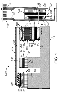
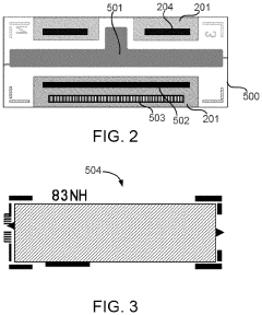
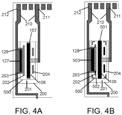
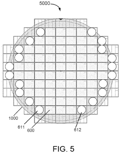
Silicon photonics light source
PatentActiveUS20220407285A1
Innovation
- A no-wirebond chip platform with a silicon photonics light source that includes a die with a trench region and a stopper region, where a laser diode chip is flip-bonded with the p-side facing the chip site and the n-side distal, and a conductor layer connects the gain region to anode and cathode electrodes, enabling wafer-level burn-in and testing.
In-situ ring-resonator-modulator calibration
PatentActiveUS20180259797A1
Innovation
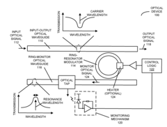
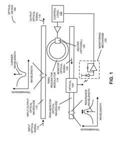
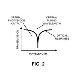
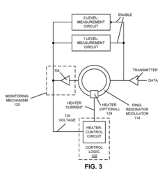
- An optical device with a ring-resonator modulator having an adjustable resonance wavelength, monitored by a ring-monitor optical waveguide and controlled by a mechanism that adjusts the resonance wavelength based on performance metrics such as average optical power or signal swing, using techniques like thermal tuning or carrier injection to optimize performance.
Photonics Integration Trends
The integration of photonics in silicon-based technologies has been a significant trend in recent years, driven by the need for faster and more efficient communication systems. This trend is particularly evident in the development of silicon photonics, which combines the advantages of optical communication with the scalability and cost-effectiveness of silicon-based manufacturing processes.
One of the key drivers of photonics integration is the increasing demand for high-bandwidth, low-latency communication in data centers and telecommunications networks. As data traffic continues to grow exponentially, traditional electronic interconnects are reaching their limits in terms of speed and power efficiency. Silicon photonics offers a promising solution by enabling the transmission of data using light, which can travel faster and with less energy loss compared to electrical signals.
The integration of photonics components on silicon chips has progressed rapidly, with advancements in areas such as on-chip lasers, modulators, and photodetectors. These developments have led to the creation of compact, high-performance optical transceivers that can be integrated directly into electronic circuits. This level of integration not only reduces the overall size and cost of communication systems but also improves their performance and reliability.
Another significant trend in photonics integration is the development of multi-chip modules (MCMs) that combine electronic and photonic components. These hybrid systems leverage the strengths of both technologies, allowing for seamless integration of high-speed optical interconnects with advanced electronic processing capabilities. This approach is particularly beneficial for applications requiring both high-bandwidth communication and complex data processing, such as artificial intelligence and high-performance computing.
The trend towards increased photonics integration is also evident in the emergence of new manufacturing techniques and materials. For example, researchers are exploring the use of novel materials like graphene and other 2D materials to create ultra-thin, highly efficient photonic devices. Additionally, advanced packaging technologies are being developed to enable the integration of photonic and electronic components in three-dimensional structures, further increasing the density and performance of integrated systems.
As photonics integration continues to advance, we can expect to see a growing convergence of optical and electronic technologies across a wide range of applications. This trend is likely to lead to the development of new types of integrated circuits that seamlessly combine photonic and electronic functionalities, paving the way for next-generation communication systems and computing architectures that can meet the ever-increasing demands for speed, efficiency, and scalability.
Energy Efficiency Impact
Silicon photonics technology has a significant impact on energy efficiency in communication systems. By integrating optical components onto silicon chips, this technology enables the transmission of data using light instead of electrical signals, resulting in substantial energy savings. The reduction in power consumption is particularly notable in data centers and high-performance computing environments, where communication latency and energy efficiency are critical concerns.
One of the primary advantages of silicon photonics is its ability to transmit data over longer distances with minimal signal degradation. This characteristic allows for more efficient data transfer between different parts of a system or between multiple systems, reducing the need for frequent signal regeneration and amplification. As a result, the overall energy consumption of the communication infrastructure is significantly lowered.
Furthermore, silicon photonics enables higher data rates with lower power consumption compared to traditional electronic interconnects. The use of light for data transmission eliminates the resistive losses associated with electrical signals, leading to improved energy efficiency. This is particularly beneficial in scenarios where large volumes of data need to be transferred quickly, such as in cloud computing and big data applications.
The integration of photonic components with electronic circuits on the same chip also contributes to energy savings. By reducing the need for separate optical and electronic components, silicon photonics minimizes the energy lost in signal conversion between optical and electrical domains. This integration also leads to more compact designs, further improving energy efficiency through reduced cooling requirements.
In addition to direct energy savings, silicon photonics indirectly contributes to overall system efficiency. The technology's ability to handle higher bandwidth with lower latency allows for more efficient data processing and computation. This, in turn, leads to reduced processing time and energy consumption in data-intensive applications, such as artificial intelligence and machine learning.
As silicon photonics technology continues to mature, its energy efficiency benefits are expected to become even more pronounced. Ongoing research and development efforts are focused on further improving the power efficiency of photonic components and their integration with electronic circuits. These advancements promise to drive down the energy consumption of communication systems even further, making silicon photonics a key enabler of sustainable and high-performance computing infrastructure.
Unlock deeper insights with Patsnap Eureka Quick Research — get a full tech report to explore trends and direct your research. Try now!
Generate Your Research Report Instantly with AI Agent
Supercharge your innovation with Patsnap Eureka AI Agent Platform!