Role of silicon photonics in wireless sensor networks.
JUL 17, 20259 MIN READ
Generate Your Research Report Instantly with AI Agent
Patsnap Eureka helps you evaluate technical feasibility & market potential.
Silicon Photonics Evolution
Silicon photonics has undergone a remarkable evolution since its inception in the late 1980s. Initially conceived as a means to integrate optical components with electronic circuits, the field has grown exponentially, driven by the increasing demand for high-speed data transmission and processing. The evolution of silicon photonics can be traced through several key phases, each marked by significant technological advancements and expanding applications.
In the early stages, researchers focused on developing basic building blocks such as waveguides, modulators, and detectors on silicon substrates. The 1990s saw the emergence of silicon-on-insulator (SOI) technology, which provided a platform for low-loss optical waveguides and became the foundation for future developments. The turn of the millennium brought about a surge in research activities, with major breakthroughs in high-speed modulators and photodetectors.
The mid-2000s marked a turning point for silicon photonics, as it began to transition from academic research to industrial applications. Companies like Intel and IBM started investing heavily in the technology, recognizing its potential to address the bandwidth limitations of traditional electronic interconnects. This period saw the development of more complex photonic integrated circuits (PICs) and the first commercial products, primarily aimed at data center applications.
As the field matured, the focus shifted towards improving performance, reducing power consumption, and enhancing integration density. Advanced manufacturing techniques, such as CMOS-compatible processes, enabled the production of silicon photonic devices at scale. This led to the development of transceivers capable of data rates exceeding 100 Gbps, a significant milestone for the industry.
In recent years, silicon photonics has expanded beyond its traditional domain of data communications. The technology has found applications in diverse fields such as biosensing, lidar for autonomous vehicles, and quantum computing. The integration of new materials, such as III-V semiconductors and 2D materials, with silicon platforms has opened up new possibilities for enhanced functionality and performance.
The evolution of silicon photonics has also been characterized by increasing miniaturization and integration. Modern PICs can incorporate hundreds of optical components on a single chip, rivaling the complexity of electronic integrated circuits. This level of integration has paved the way for novel architectures in computing and communication systems, including optical neural networks and photonic quantum processors.
In the context of wireless sensor networks, silicon photonics has emerged as a promising technology for addressing the challenges of power efficiency, bandwidth, and latency. The ability to integrate optical and electronic components on a single chip offers unique opportunities for developing compact, low-power sensor nodes with enhanced communication capabilities. As silicon photonics continues to evolve, it is poised to play an increasingly important role in shaping the future of wireless sensor networks and other emerging technologies.
WSN Market Demand Analysis
The wireless sensor network (WSN) market has been experiencing significant growth and transformation, driven by the increasing demand for IoT applications across various industries. The integration of silicon photonics in WSNs presents a promising opportunity to address several key market needs and challenges.
One of the primary market demands for WSNs is improved energy efficiency and extended battery life. Traditional WSN nodes often face limitations in power consumption, which restricts their deployment in remote or hard-to-reach locations. Silicon photonics offers a potential solution by enabling low-power optical communication links, reducing the overall energy requirements of sensor nodes. This aligns with the market's need for long-lasting, maintenance-free WSN deployments.
Another crucial market demand is increased data transmission rates and network capacity. As IoT applications become more sophisticated, there is a growing need for WSNs to handle larger volumes of data with minimal latency. Silicon photonics can significantly enhance the bandwidth capabilities of WSNs, allowing for faster and more efficient data transfer between nodes and gateways. This improvement in network performance is particularly valuable in applications such as industrial automation, smart cities, and environmental monitoring.
The market also seeks enhanced reliability and robustness in WSN deployments. Silicon photonics can contribute to this demand by providing immunity to electromagnetic interference, which is a common challenge in traditional radio frequency-based WSNs. This characteristic makes silicon photonic-enabled WSNs particularly attractive for deployment in harsh industrial environments or areas with high electromagnetic noise.
Miniaturization and cost-effectiveness are additional market requirements that silicon photonics can address. The ability to integrate optical components on a silicon chip allows for smaller, more compact WSN nodes. This miniaturization not only reduces the overall cost of deployment but also enables new applications in space-constrained environments.
The healthcare and biomedical sectors represent a growing market segment for WSNs, with increasing demand for wearable and implantable sensors. Silicon photonics can enable the development of highly sensitive, miniaturized biosensors that can be integrated into WSNs for continuous health monitoring and early disease detection.
In the agricultural sector, there is a rising demand for precision farming techniques that rely on extensive sensor networks. Silicon photonic-enabled WSNs can offer improved sensing capabilities and data transmission, allowing farmers to monitor crop health, soil conditions, and environmental factors more accurately and in real-time.
The smart city market segment also presents significant opportunities for silicon photonic WSNs. With the increasing focus on urban infrastructure management and environmental monitoring, there is a growing need for large-scale, energy-efficient sensor networks that can provide real-time data on air quality, traffic conditions, and energy consumption.
Current Challenges in WSN
Wireless Sensor Networks (WSNs) have revolutionized data collection and monitoring across various industries. However, as the demand for more sophisticated and efficient WSNs grows, several challenges have emerged that hinder their widespread adoption and optimal performance.
One of the primary challenges facing WSNs is energy efficiency. Sensor nodes are typically battery-powered, and their limited energy resources significantly constrain their operational lifespan. This limitation becomes particularly acute in large-scale deployments or in environments where frequent battery replacement is impractical or costly.
Data transmission reliability presents another significant hurdle. WSNs often operate in harsh or unpredictable environments, leading to signal interference, packet loss, and communication failures. These issues can result in incomplete or inaccurate data collection, potentially compromising the integrity of the entire network.
Scalability remains a persistent challenge for WSNs. As networks grow in size and complexity, issues such as increased latency, reduced throughput, and heightened energy consumption become more pronounced. Efficiently managing and coordinating large numbers of sensor nodes while maintaining network performance is a complex task that requires innovative solutions.
Security and privacy concerns also pose significant challenges in WSN deployments. The wireless nature of these networks makes them vulnerable to various cyber attacks, including eavesdropping, data manipulation, and denial of service attacks. Implementing robust security measures without significantly impacting network performance or energy consumption is a delicate balancing act.
The heterogeneity of sensor nodes and network protocols adds another layer of complexity to WSNs. Integrating diverse sensors, each with its own data formats, communication protocols, and operational requirements, into a cohesive and efficient network remains a challenging task. This diversity can lead to interoperability issues and complicate network management and data aggregation processes.
Resource constraints, particularly in terms of processing power and memory, limit the capabilities of individual sensor nodes. This restriction impacts the complexity of algorithms that can be implemented on these nodes, potentially affecting data processing, encryption, and decision-making capabilities at the edge of the network.
Environmental factors pose unique challenges for WSNs deployed in harsh or remote locations. Extreme temperatures, humidity, electromagnetic interference, and physical obstacles can all impact the performance and longevity of sensor nodes. Designing robust hardware and adaptive networking protocols to withstand these conditions is crucial for ensuring reliable long-term operation.
As WSNs evolve to support more complex applications, the need for real-time data processing and decision-making becomes increasingly important. However, achieving low-latency, high-throughput communication while maintaining energy efficiency presents a significant technical challenge, particularly in large-scale or geographically dispersed networks.
Si-Photonics Solutions for WSN
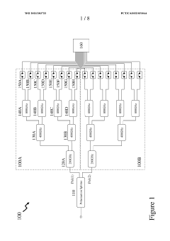
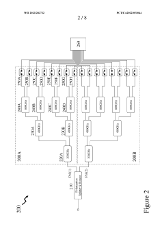
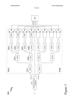
01 Optical interconnects and communication systems
Silicon photonics technology is utilized in developing high-speed optical interconnects and communication systems. These systems integrate optical components on silicon chips, enabling efficient data transmission and processing in various applications, including telecommunications and data centers.- Integrated photonic devices: Silicon photonics technology enables the integration of various optical components on a single chip. This includes waveguides, modulators, detectors, and other photonic elements, allowing for compact and efficient optical systems. The integration of these components facilitates high-speed data transmission and processing in a small form factor.
- Optical communication systems: Silicon photonics is extensively used in optical communication systems to enhance data transmission capabilities. This technology enables the development of high-bandwidth interconnects, transceivers, and optical switches, which are crucial for next-generation data centers and telecommunications networks. The use of silicon photonics in these systems allows for faster and more efficient data transfer.
- Photonic integrated circuits (PICs): Silicon photonics technology is used to create advanced photonic integrated circuits. These PICs combine multiple optical functions on a single chip, including light generation, modulation, detection, and routing. The integration of these functions enables complex optical processing and sensing applications, while reducing size, power consumption, and cost compared to discrete optical components.
- Silicon-based light sources and detectors: Advancements in silicon photonics have led to the development of efficient light sources and detectors integrated on silicon chips. This includes the integration of III-V materials with silicon to create lasers and the development of high-performance photodetectors. These components are essential for creating fully integrated photonic systems on silicon platforms.
- Photonic computing and signal processing: Silicon photonics technology is being applied to develop photonic computing and signal processing systems. This includes the creation of optical neural networks, photonic accelerators for artificial intelligence, and optical signal processing units. These applications leverage the high speed and parallelism of light to perform computations and process signals more efficiently than traditional electronic systems.
02 Integration of photonic and electronic components
Silicon photonics allows for the integration of photonic and electronic components on a single chip. This integration enables the development of compact, energy-efficient devices that combine the benefits of both optical and electronic technologies, leading to improved performance in various applications.Expand Specific Solutions03 Waveguide structures and optical modulators
Silicon photonics technology involves the development of advanced waveguide structures and optical modulators. These components are crucial for manipulating light signals within integrated photonic circuits, enabling efficient signal routing, modulation, and processing.Expand Specific Solutions04 Photonic integrated circuits for quantum computing
Silicon photonics is being applied to develop photonic integrated circuits for quantum computing applications. These circuits leverage the properties of light to perform quantum operations, potentially enabling more powerful and scalable quantum computing systems.Expand Specific Solutions05 Silicon-based light sources and detectors
Research in silicon photonics focuses on developing efficient silicon-based light sources and detectors. These components are essential for creating fully integrated photonic systems on silicon chips, overcoming the limitations of silicon's indirect bandgap and enabling a wide range of applications in sensing and communication.Expand Specific Solutions
Key Players in Si-Photonics
The role of silicon photonics in wireless sensor networks is evolving within a competitive landscape characterized by rapid technological advancements and growing market potential. The industry is in a transitional phase, moving from research and development to early commercialization. The market size is expanding, driven by increasing demand for high-speed, energy-efficient communication in IoT applications. Technologically, silicon photonics is maturing, with key players like Huawei, IBM, and Marvell making significant strides. Research institutions such as CNRS, IMEC, and universities like Zhejiang and Ghent are contributing to innovation. Companies like Ciena and Toshiba are exploring integration possibilities, while startups are emerging with specialized solutions, indicating a dynamic and diversifying ecosystem.
Huawei Technologies Co., Ltd.
Technical Solution: Huawei has developed a silicon photonics-based solution for wireless sensor networks that integrates optical transceivers and sensors on a single chip. This approach leverages the high bandwidth and low power consumption of silicon photonics to enable efficient data transmission in WSNs. The company's technology utilizes wavelength division multiplexing (WDM) to support multiple sensor nodes on a single optical fiber, significantly reducing network complexity and power requirements[1]. Huawei's silicon photonic sensors can detect various environmental parameters such as temperature, pressure, and chemical composition with high sensitivity and accuracy[2].
Strengths: High integration, low power consumption, and scalability. Weaknesses: Potentially higher initial costs and complexity in deployment compared to traditional WSN solutions.
International Business Machines Corp.
Technical Solution: IBM has developed a silicon photonics platform for wireless sensor networks that focuses on edge computing and AI integration. Their solution combines high-speed optical interconnects with on-chip processing capabilities, enabling real-time data analysis at the sensor node level[7]. IBM's technology utilizes dense wavelength division multiplexing (DWDM) to support high-bandwidth communication between sensor nodes and central processing units. The company has also developed advanced photonic neural network architectures that can be integrated into WSN nodes, enabling efficient machine learning operations directly on the sensor data[8].
Strengths: Advanced edge computing capabilities, high-speed data processing, and AI integration. Weaknesses: Potentially higher power consumption and complexity in node design.
Core Si-Photonics Innovations
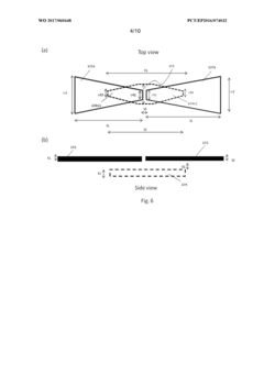
Switched wavelength optical receiver for direct-detection methods and systems
PatentWO2023283722A1
Innovation
- A switched wavelength optical receiver is implemented, comprising a series of wavelength selective optical switch elements with progressively doubling free spectral range, coupled with polarization management and photodetectors, allowing dynamic selection of wavelength channels and mitigating polarization dependency through cascaded deinterleaving and optical switching.
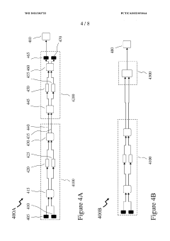
Optical coupling scheme
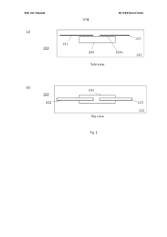
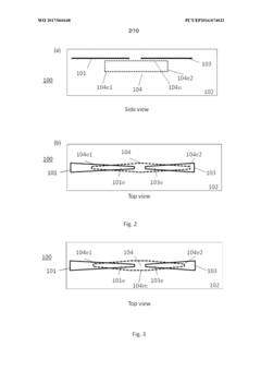
PatentWO2017060448A1
Innovation
- A waveguide structure with a first waveguide of refractive index ≤ 3, an intermediate waveguide, and a second waveguide of higher refractive index, arranged to enable adiabatic optical coupling, using a silicon-on-insulator wafer substrate and CMOS-compatible processes to reduce manufacturing steps and costs.

Energy Efficiency in WSN
Energy efficiency is a critical aspect of wireless sensor networks (WSNs) due to the limited power resources available to sensor nodes. In the context of silicon photonics integration, several innovative approaches have been developed to enhance energy efficiency in WSNs.
One of the primary methods for improving energy efficiency is through the use of silicon photonic transceivers. These devices leverage the low-loss transmission properties of silicon waveguides to reduce power consumption in data transmission and reception. By integrating photonic components directly onto silicon chips, the overall power requirements for communication within the network can be significantly reduced.
Silicon photonics also enables the implementation of wavelength division multiplexing (WDM) in WSNs. This technique allows multiple data streams to be transmitted simultaneously over a single optical fiber, increasing the overall bandwidth while minimizing energy consumption. The use of WDM can lead to more efficient data aggregation and transmission, reducing the number of active communication cycles required for each sensor node.
Another area where silicon photonics contributes to energy efficiency is in the development of low-power optical sensors. These sensors can detect various environmental parameters with high sensitivity while consuming minimal energy. By integrating such sensors directly into the silicon photonic platform, the need for separate sensing and communication modules is eliminated, further reducing power requirements.
The integration of silicon photonics in WSNs also facilitates the implementation of energy harvesting techniques. Photovoltaic cells can be integrated onto the same silicon substrate as the photonic components, allowing sensor nodes to generate their own power from ambient light. This approach can significantly extend the operational lifetime of WSN nodes, reducing the need for battery replacements and maintenance.
Furthermore, silicon photonics enables the development of all-optical switching and routing mechanisms within WSNs. These systems can operate with lower power consumption compared to traditional electronic switches, leading to improved energy efficiency in network topology management and data routing.
In conclusion, the role of silicon photonics in enhancing energy efficiency in WSNs is multifaceted, encompassing improvements in communication, sensing, power generation, and network management. As the technology continues to advance, it is expected to play an increasingly important role in the development of sustainable and long-lasting wireless sensor networks.
Scalability of Si-Photonics WSN
The scalability of silicon photonics in wireless sensor networks (WSNs) presents a promising avenue for addressing the growing demands of IoT applications. As sensor networks expand in size and complexity, traditional electronic systems face limitations in terms of power consumption, bandwidth, and integration density. Silicon photonics offers a potential solution to these challenges by leveraging the advantages of optical communication within the compact and cost-effective silicon platform.
One of the key factors contributing to the scalability of Si-photonics WSNs is the ability to achieve high data rates over long distances with minimal power consumption. This is particularly crucial for large-scale sensor networks where energy efficiency is paramount. Silicon photonic devices can operate at speeds of tens of gigabits per second while consuming only a fraction of the power required by their electronic counterparts. This enables the deployment of more sensors over wider areas without compromising network performance or battery life.
Another aspect of scalability lies in the integration capabilities of silicon photonics. The compatibility with CMOS fabrication processes allows for the seamless integration of photonic components with electronic circuits on a single chip. This level of integration facilitates the development of compact, multi-functional sensor nodes that can incorporate various sensing modalities alongside communication capabilities. As a result, WSNs can be scaled up in terms of both node count and functionality without significantly increasing the overall system size or complexity.
The wavelength division multiplexing (WDM) capabilities of silicon photonics further enhance the scalability of WSNs. By utilizing multiple wavelengths of light, a single optical fiber or waveguide can carry multiple data streams simultaneously. This dramatically increases the overall bandwidth capacity of the network, allowing for the accommodation of a larger number of sensors and higher data throughput. The ability to scale bandwidth through WDM is particularly valuable in scenarios where sensor density is high or where real-time data processing is required.
Moreover, the low-loss characteristics of silicon photonic waveguides enable the implementation of long-range optical links within WSNs. This reduces the need for frequent signal regeneration or amplification, simplifying network topology and improving overall system reliability. As WSNs expand geographically, the extended reach of silicon photonic links can help maintain network connectivity without the need for additional intermediate nodes or complex routing schemes.
The scalability of Si-photonics WSNs also extends to the realm of data processing and analysis. The high-speed optical interconnects facilitated by silicon photonics can support the rapid transfer of large volumes of sensor data to centralized processing units or edge computing nodes. This enables real-time analysis and decision-making, even as the network scales to encompass thousands or millions of sensors. The ability to handle increasing data loads without compromising processing speed is crucial for applications such as environmental monitoring, smart cities, and industrial IoT.
Unlock deeper insights with Patsnap Eureka Quick Research — get a full tech report to explore trends and direct your research. Try now!
Generate Your Research Report Instantly with AI Agent
Supercharge your innovation with Patsnap Eureka AI Agent Platform!