

Silicon photonics for next-generation data collection methodologies.
JUL 17, 20259 MIN READ
Generate Your Research Report Instantly with AI Agent
Patsnap Eureka helps you evaluate technical feasibility & market potential.
Silicon Photonics Evolution and Objectives
Silicon photonics has emerged as a transformative technology in the field of data collection and processing, offering unprecedented capabilities for high-speed, low-power, and high-density integrated photonic circuits. The evolution of this technology can be traced back to the early 2000s when researchers first began exploring the potential of integrating photonic components with silicon-based electronic circuits.
The initial objectives of silicon photonics were primarily focused on overcoming the limitations of traditional electronic interconnects in data centers and high-performance computing systems. As data rates continued to increase, the need for faster and more efficient communication became paramount. Silicon photonics promised to address these challenges by leveraging the high-speed capabilities of light for data transmission while maintaining compatibility with existing CMOS fabrication processes.
Over the past two decades, silicon photonics has made significant strides in achieving its early objectives. The technology has successfully demonstrated the integration of various photonic components, including waveguides, modulators, detectors, and lasers, on a single silicon chip. This integration has led to dramatic improvements in data transmission speeds, power efficiency, and overall system performance.
As the field has matured, the objectives of silicon photonics have expanded beyond mere interconnects. Today, the technology aims to revolutionize a wide range of applications, including next-generation data collection methodologies. The current goals include developing ultra-high-bandwidth optical interconnects, creating compact and energy-efficient sensors for IoT and edge computing, and enabling advanced quantum computing and communication systems.
In the context of next-generation data collection, silicon photonics is poised to play a crucial role. The technology's ability to manipulate light at the nanoscale opens up new possibilities for high-precision sensing and data acquisition. Objectives in this area include developing integrated photonic circuits capable of collecting and processing vast amounts of data in real-time, with applications ranging from environmental monitoring to biomedical diagnostics.
Looking ahead, the future objectives of silicon photonics in data collection methodologies are ambitious and far-reaching. Researchers are working towards achieving even higher levels of integration, with the ultimate goal of creating fully photonic systems-on-chip that can handle both data collection and processing entirely in the optical domain. This would enable unprecedented speeds and efficiencies in data handling, potentially revolutionizing fields such as artificial intelligence, machine learning, and big data analytics.
Data Collection Market Demand Analysis
The market demand for advanced data collection methodologies is experiencing significant growth, driven by the exponential increase in data generation and the need for faster, more efficient data processing. Silicon photonics technology is emerging as a key enabler for next-generation data collection systems, offering unprecedented speed, bandwidth, and energy efficiency.
In the telecommunications sector, the demand for high-speed data transmission is surging due to the proliferation of 5G networks and the increasing adoption of cloud computing services. Silicon photonics-based data collection systems can provide the necessary bandwidth to support these applications, with potential data rates exceeding 100 Gbps per channel. This capability is crucial for meeting the growing demand for real-time data processing and low-latency communication.
The data center industry is another major driver of market demand for silicon photonics-based data collection solutions. As data centers continue to expand and handle ever-increasing volumes of information, there is a pressing need for more efficient data collection and transmission technologies. Silicon photonics offers the potential to significantly reduce power consumption and increase data throughput within data centers, addressing critical challenges faced by operators in terms of energy efficiency and scalability.
In the field of scientific research and high-performance computing, silicon photonics is poised to revolutionize data collection methodologies. Applications such as particle physics experiments, genomics research, and climate modeling require the ability to collect and process massive amounts of data in real-time. Silicon photonics-based systems can provide the necessary speed and bandwidth to support these demanding applications, enabling breakthroughs in scientific discovery and analysis.
The healthcare sector is also showing increasing interest in silicon photonics for data collection. As medical imaging technologies advance and telemedicine becomes more prevalent, there is a growing need for high-speed, high-fidelity data transmission systems. Silicon photonics can enable faster and more accurate transmission of medical images and real-time patient data, potentially improving diagnostic capabilities and patient outcomes.
In the automotive industry, the development of autonomous vehicles is driving demand for advanced sensor systems and data collection technologies. Silicon photonics-based LiDAR systems offer the potential for higher resolution, longer range, and faster data processing compared to traditional sensor technologies. This capability is crucial for enabling safe and reliable autonomous driving in various environmental conditions.
The market for silicon photonics in data collection applications is expected to grow significantly in the coming years. While specific market size projections vary, industry analysts consistently predict double-digit growth rates for the silicon photonics market, with data collection and transmission being key application areas driving this growth. As the technology matures and manufacturing processes improve, the adoption of silicon photonics-based data collection systems is likely to accelerate across multiple industries, further expanding the market opportunity.
Current Challenges in Silicon Photonics
Silicon photonics has made significant strides in recent years, yet several challenges persist in its development and implementation for next-generation data collection methodologies. One of the primary obstacles is the integration of photonic components with traditional electronic circuits. While silicon photonics offers high-speed data transmission and processing capabilities, seamlessly interfacing these optical elements with existing electronic systems remains complex and costly.
Another critical challenge lies in the miniaturization of photonic components. As data centers and communication networks demand ever-increasing bandwidth and efficiency, there is a pressing need to reduce the size of photonic devices while maintaining or improving their performance. This miniaturization effort is particularly challenging due to the fundamental limitations of light propagation and the difficulties in confining light to extremely small dimensions.
The issue of thermal management also poses a significant hurdle in silicon photonics. As photonic circuits become more densely packed and operate at higher speeds, heat generation becomes a major concern. Excessive heat can lead to performance degradation and reliability issues, necessitating innovative cooling solutions that are compatible with the delicate nature of photonic components.
Furthermore, the manufacturing processes for silicon photonic devices still face challenges in terms of yield and consistency. The precision required for fabricating photonic structures at the nanoscale is extremely high, and even minor variations can significantly impact device performance. Achieving high-volume, cost-effective production of silicon photonic components with consistent quality remains an ongoing challenge for the industry.
Another area of concern is the development of efficient and reliable light sources integrated directly onto silicon chips. While progress has been made in this direction, creating high-performance lasers on silicon substrates continues to be a technical hurdle due to the indirect bandgap nature of silicon.
Additionally, the field of silicon photonics faces challenges in developing robust and efficient modulation techniques for high-speed data transmission. Current modulation schemes often suffer from limitations in speed, power consumption, or signal quality, necessitating further research and innovation to meet the demands of next-generation data collection systems.
Lastly, the standardization of silicon photonic components and interfaces remains an ongoing challenge. The lack of widely accepted industry standards can hinder interoperability and slow down the adoption of silicon photonics in various applications. Establishing common protocols and specifications for silicon photonic devices and systems is crucial for the technology's widespread implementation in data collection and communication infrastructures.
Existing Silicon Photonics Solutions
01 Integrated photonic devices
Silicon photonics technology enables the integration of various optical components on a single chip. This includes waveguides, modulators, detectors, and other photonic elements, allowing for compact and efficient optical systems. The integration of these components facilitates high-speed data transmission and processing in optical communication networks and computing applications.- Optical interconnects and communication systems: Silicon photonics technology is utilized in developing high-speed optical interconnects and communication systems. These systems integrate optical components on silicon chips, enabling efficient data transmission and processing in various applications, including data centers and telecommunications networks.
- Integration of photonic and electronic components: Silicon photonics allows for the integration of photonic and electronic components on a single chip. This integration enables the development of compact, energy-efficient devices that combine the benefits of both optical and electronic technologies, leading to improved performance in various applications.
- Waveguide structures and optical modulators: Advanced waveguide structures and optical modulators are key components in silicon photonics. These elements are designed to efficiently guide and manipulate light on silicon chips, enabling high-speed data transmission and signal processing in photonic integrated circuits.
- Photonic sensors and detectors: Silicon photonics technology is applied in the development of highly sensitive photonic sensors and detectors. These devices leverage the properties of silicon to create compact, efficient sensors for various applications, including environmental monitoring, biomedical sensing, and industrial process control.
- Quantum photonics and computing: Silicon photonics plays a crucial role in advancing quantum photonics and computing technologies. By integrating quantum light sources, manipulators, and detectors on silicon chips, researchers are developing scalable platforms for quantum information processing and communication.
02 Optical interconnects
Silicon photonics is utilized in developing optical interconnects for high-speed data transfer between chips or within computer systems. These interconnects use light for data transmission, offering advantages such as higher bandwidth, lower power consumption, and reduced latency compared to traditional electrical interconnects. This technology is crucial for addressing bandwidth limitations in data centers and high-performance computing systems.Expand Specific Solutions03 Photonic integrated circuits (PICs)
Silicon photonics enables the development of photonic integrated circuits, which combine multiple optical functions on a single chip. These PICs can include lasers, modulators, multiplexers, and detectors, all integrated on a silicon substrate. This integration allows for complex optical processing and routing capabilities, essential for applications in telecommunications, sensing, and quantum computing.Expand Specific Solutions04 Silicon-based light sources
Developing efficient light sources on silicon platforms is a key area of silicon photonics research. This includes the integration of III-V materials on silicon for laser generation, as well as the development of silicon-based light emitters. These advancements aim to overcome the indirect bandgap limitation of silicon and enable fully integrated photonic systems on a silicon platform.Expand Specific Solutions05 Photonic computing and AI acceleration
Silicon photonics is being explored for photonic computing applications, including optical neural networks and AI acceleration. By leveraging the properties of light for computation, these systems aim to achieve higher processing speeds and energy efficiency compared to traditional electronic systems. This includes the development of photonic tensor cores and optical matrix multiplication units for machine learning applications.Expand Specific Solutions
Key Players in Silicon Photonics Industry
The silicon photonics market for next-generation data collection methodologies is in a growth phase, with increasing adoption across various industries. The market size is expanding rapidly, driven by the demand for high-speed data transmission and processing capabilities. Technologically, silicon photonics is maturing, with key players like Intel, IBM, and Huawei making significant advancements. Companies such as GlobalFoundries and TSMC are developing manufacturing processes to scale production. Academic institutions like MIT and Zhejiang University are contributing to fundamental research, while industry leaders like Corning and Ciena are focusing on practical applications. The competitive landscape is diverse, with both established tech giants and specialized startups like Aeponyx vying for market share in this promising field.
International Business Machines Corp.
Technical Solution: IBM has developed a silicon photonics platform that integrates both electronic and photonic components on a single chip. Their technology uses sub-100nm manufacturing processes to create high-performance, energy-efficient photonic integrated circuits. IBM's approach includes on-chip optical transceivers capable of transmitting data at speeds up to 100 Gbps per channel[1]. They have also demonstrated a fully integrated wavelength-division multiplexing (WDM) system on a single chip, allowing for multiple data streams to be transmitted simultaneously over a single optical fiber[2]. This technology enables next-generation data centers to handle massive amounts of data with reduced power consumption and improved bandwidth.
Strengths: High integration level, scalable manufacturing process, and compatibility with existing CMOS technology. Weaknesses: Potential challenges in thermal management and coupling efficiency between electronic and photonic components.
Taiwan Semiconductor Manufacturing Co., Ltd.
Technical Solution: TSMC's silicon photonics technology leverages their advanced semiconductor manufacturing processes to create high-performance, integrated photonic circuits. They have developed a silicon photonics platform that includes passive and active components such as waveguides, modulators, and photodetectors. TSMC's approach focuses on monolithic integration of photonic and electronic components using their state-of-the-art CMOS processes, including 7nm and 5nm nodes[9]. This enables the production of compact, energy-efficient photonic integrated circuits suitable for next-generation data collection and processing applications. TSMC has also demonstrated the ability to integrate III-V lasers with their silicon photonics platform through advanced bonding techniques, enabling on-chip light generation[10].
Strengths: World-leading semiconductor manufacturing capabilities. Ability to leverage advanced CMOS processes for photonic integration. Weaknesses: Less experience in system-level optical networking compared to some specialized photonics companies.
Core Innovations in Silicon Photonics
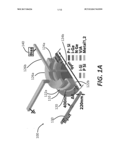
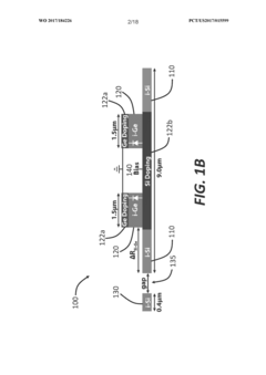
Apparatus, systems, and methods for waveguide-coupled resonant photon detection
PatentWO2017184226A1
Innovation
- A germanium layer is evanescently coupled to a resonator, allowing for extended interaction length without increasing detector size, with a bias voltage applied to convert absorbed light into electrical signals, and the internal and external quality factors of the resonator are matched for high quantum efficiency.

Integration with AI and Machine Learning
The integration of silicon photonics with AI and machine learning presents a transformative opportunity for next-generation data collection methodologies. This synergy leverages the high-speed, low-latency capabilities of silicon photonics alongside the powerful data processing and decision-making abilities of AI systems.
Silicon photonics enables the transmission and processing of optical signals on integrated circuits, offering unprecedented bandwidth and energy efficiency. When combined with AI and machine learning algorithms, this technology can significantly enhance data collection, analysis, and real-time decision-making processes.
One key application area is in high-performance computing and data centers. AI-driven silicon photonic interconnects can optimize data routing and processing, reducing latency and improving overall system performance. Machine learning algorithms can dynamically adjust optical signal parameters to adapt to changing network conditions, ensuring optimal data transmission rates and quality.
In the realm of sensor networks and Internet of Things (IoT) devices, silicon photonics integrated with AI can enable more intelligent and efficient data collection. AI algorithms can process raw optical data at the edge, reducing the amount of information that needs to be transmitted to central servers. This approach not only conserves bandwidth but also enhances privacy and security by minimizing data movement.
The integration also opens up new possibilities in quantum computing and communication. AI can assist in the calibration and control of silicon photonic quantum devices, improving qubit stability and reducing error rates. Machine learning algorithms can be employed to optimize quantum circuit designs and enhance the performance of quantum photonic systems.
In the field of biomedical imaging and diagnostics, AI-enhanced silicon photonic systems can enable real-time analysis of optical signals from biological samples. This integration can lead to more accurate and faster disease detection, personalized medicine, and non-invasive monitoring of physiological parameters.
However, challenges remain in fully realizing the potential of this integration. These include developing efficient interfaces between photonic and electronic components, optimizing AI algorithms for photonic hardware, and addressing the complexities of manufacturing hybrid photonic-electronic systems at scale.
As research progresses, we can expect to see more sophisticated AI-driven silicon photonic systems that push the boundaries of data collection and processing capabilities. This integration will likely play a crucial role in shaping the future of computing, communications, and sensing technologies.
Environmental Impact and Sustainability
Silicon photonics technology, while offering significant advantages in data collection and processing, also presents important environmental considerations. The production of silicon photonic devices involves complex manufacturing processes that can have substantial environmental impacts. These processes often require the use of rare earth elements and other precious materials, which may lead to resource depletion and environmental degradation in mining areas.
However, the energy efficiency of silicon photonics in data transmission and processing can potentially offset some of these environmental costs. Compared to traditional electronic systems, silicon photonic devices consume less power and generate less heat, reducing the overall energy demand of data centers and communication networks. This efficiency gain could contribute to lowering greenhouse gas emissions associated with the rapidly growing digital infrastructure.
The miniaturization capabilities of silicon photonics also play a role in sustainability. Smaller, more efficient devices mean less material usage and potentially longer lifespans for electronic products. This could help reduce electronic waste, a growing environmental concern in the tech industry. Additionally, the improved performance of silicon photonic devices in data collection methodologies may enable more accurate environmental monitoring and management systems, indirectly contributing to sustainability efforts.
Despite these potential benefits, the end-of-life management of silicon photonic devices remains a challenge. The complex integration of optical and electronic components can make recycling difficult, potentially contributing to e-waste issues. Research into design for disassembly and recycling of these devices is crucial for improving their overall environmental footprint.
The water usage in the manufacturing process of silicon photonic devices is another environmental concern. Semiconductor fabrication requires significant amounts of ultra-pure water, which can strain local water resources, especially in water-scarce regions. Developing more water-efficient manufacturing processes and implementing water recycling systems in production facilities are important steps towards improving the sustainability of silicon photonics technology.
As the adoption of silicon photonics in next-generation data collection methodologies grows, it is essential to conduct comprehensive life cycle assessments. These assessments should consider the environmental impacts from raw material extraction through manufacturing, use, and disposal. Such analyses can guide the development of more sustainable practices in the silicon photonics industry and inform policy decisions to mitigate potential negative environmental effects.
Unlock deeper insights with Patsnap Eureka Quick Research — get a full tech report to explore trends and direct your research. Try now!
Generate Your Research Report Instantly with AI Agent
Supercharge your innovation with Patsnap Eureka AI Agent Platform!