Innovations in silicon photonics for flexible electronic devices.
JUL 17, 20259 MIN READ
Generate Your Research Report Instantly with AI Agent
Patsnap Eureka helps you evaluate technical feasibility & market potential.
Silicon Photonics Evolution
Silicon photonics has undergone a remarkable evolution since its inception in the late 1980s. Initially conceived as a means to integrate optical components with electronic circuits on silicon substrates, the field has grown exponentially, driven by the increasing demand for high-speed data transmission and processing.
The early stages of silicon photonics focused on developing basic building blocks such as waveguides, modulators, and detectors. Researchers faced significant challenges in overcoming silicon's inherent limitations as an optical material, particularly its indirect bandgap, which made light emission difficult. Despite these hurdles, the 1990s saw steady progress in fabricating low-loss waveguides and demonstrating basic optical functionalities on silicon.
The turn of the millennium marked a pivotal moment in silicon photonics evolution. Breakthroughs in fabrication techniques, particularly the adaptation of CMOS processes, enabled the integration of complex photonic circuits on silicon chips. This period witnessed the development of high-speed modulators, efficient photodetectors, and the first attempts at creating silicon-based light sources through techniques like Raman lasing.
From 2010 onwards, silicon photonics entered a phase of rapid commercialization. Major tech companies and startups alike began investing heavily in the technology, recognizing its potential to revolutionize data centers and telecommunications. This period saw the emergence of silicon photonic transceivers capable of transmitting data at unprecedented rates, paving the way for next-generation optical interconnects.
Recent years have seen a shift towards exploring novel applications of silicon photonics beyond traditional communication systems. The integration of silicon photonics with flexible electronic devices represents one of the most exciting frontiers in this evolution. Researchers are now developing techniques to fabricate photonic components on flexible substrates, opening up possibilities for wearable optical sensors, bendable displays, and advanced biomedical devices.
The evolution of silicon photonics for flexible electronics faces unique challenges, including maintaining optical performance under mechanical stress and developing fabrication processes compatible with both silicon photonics and flexible substrates. However, recent advancements in materials science and nanofabrication are steadily overcoming these obstacles, promising a new era of flexible, integrated optoelectronic devices.
Flexible Electronics Market
The flexible electronics market has been experiencing significant growth and transformation in recent years, driven by advancements in materials science, manufacturing processes, and increasing demand for lightweight, portable, and adaptable electronic devices. This market encompasses a wide range of products, including flexible displays, wearable devices, sensors, and solar cells, all of which benefit from the integration of silicon photonics and flexible substrates.
The global flexible electronics market is projected to expand rapidly, with estimates suggesting a compound annual growth rate (CAGR) of over 10% in the coming years. This growth is fueled by several factors, including the rising adoption of Internet of Things (IoT) devices, increasing consumer demand for smart wearables, and the automotive industry's shift towards more advanced, flexible electronic components.
One of the key drivers of market growth is the consumer electronics sector, where flexible displays and touch screens are becoming increasingly popular. Smartphones, tablets, and wearable devices are incorporating flexible components to enhance durability, improve user experience, and enable new form factors. The automotive industry is another significant contributor to market expansion, with flexible electronics being integrated into vehicle interiors, lighting systems, and advanced driver assistance systems (ADAS).
The healthcare sector is also emerging as a crucial market for flexible electronics, particularly in the development of wearable medical devices and biosensors. These technologies enable continuous health monitoring, drug delivery systems, and personalized medicine applications, driving demand for flexible, biocompatible electronic components.
Geographically, Asia-Pacific is expected to dominate the flexible electronics market, with countries like China, South Korea, and Japan leading in both production and consumption. North America and Europe are also significant markets, particularly in terms of research and development activities and high-end applications.
However, the market faces several challenges, including high initial production costs, technical limitations in achieving full flexibility while maintaining performance, and concerns about long-term reliability. Despite these obstacles, ongoing research and development efforts, particularly in the field of silicon photonics for flexible devices, are expected to address many of these issues and further drive market growth.
As the technology matures and production costs decrease, the flexible electronics market is poised for widespread adoption across various industries. This trend is likely to create new opportunities for innovation, particularly in the integration of silicon photonics with flexible substrates, potentially revolutionizing the way electronic devices are designed, manufactured, and used in everyday applications.
Challenges in Integration
The integration of silicon photonics into flexible electronic devices presents several significant challenges that researchers and engineers must overcome. One of the primary obstacles is the inherent rigidity of silicon, which contrasts sharply with the flexibility required for wearable and bendable electronics. This mismatch in material properties necessitates innovative approaches to maintain the performance of photonic components under various deformation conditions.
Another critical challenge lies in the thermal management of integrated photonic circuits on flexible substrates. Silicon photonic devices often generate heat during operation, and the thermal conductivity of flexible materials is typically lower than that of traditional rigid substrates. This can lead to localized heating and potential performance degradation or device failure if not properly addressed.
The fabrication processes for silicon photonics and flexible electronics are also fundamentally different, requiring careful consideration and adaptation. Traditional silicon photonics manufacturing relies on high-temperature processes and precise lithography techniques, which may not be compatible with the temperature-sensitive materials used in flexible electronics. Developing low-temperature fabrication methods and adapting existing processes to accommodate flexible substrates is crucial for successful integration.
Achieving reliable and stable optical coupling between flexible photonic components and external light sources or detectors poses another significant challenge. The dynamic nature of flexible devices can lead to misalignment and coupling losses, necessitating the development of robust and adaptive coupling mechanisms that can maintain high efficiency under various bending and stretching conditions.
The integration of active components, such as modulators and detectors, into flexible photonic circuits introduces additional complexities. These devices often require precise control of material properties and electrical connections, which can be difficult to maintain in a flexible format. Innovative designs and materials are needed to ensure the functionality and reliability of active photonic components in bendable and stretchable configurations.
Packaging and encapsulation of flexible silicon photonic devices present unique challenges compared to their rigid counterparts. The protective layers must not only shield the devices from environmental factors but also maintain flexibility without compromising optical performance. Developing suitable encapsulation materials and techniques that can withstand repeated bending and stretching cycles while preserving the integrity of the photonic components is essential for long-term device reliability.
Lastly, the integration of silicon photonics with other flexible electronic components, such as sensors, antennas, and power sources, requires careful consideration of system-level design and compatibility. Ensuring seamless interaction between photonic and electronic elements while maintaining overall flexibility and performance is a complex task that demands interdisciplinary approaches and novel integration strategies.
Current Integration Tech
01 Flexible silicon photonic devices
Development of flexible silicon photonic devices that can be bent or curved without compromising their optical performance. These devices incorporate innovative materials and structures to achieve flexibility while maintaining the advantages of silicon photonics, such as high integration density and compatibility with existing semiconductor manufacturing processes.- Flexible silicon photonic devices: Development of flexible silicon photonic devices that can be bent or curved without compromising their optical performance. These devices incorporate novel materials and structures to achieve flexibility while maintaining the advantages of silicon photonics, such as high integration density and compatibility with existing semiconductor manufacturing processes.
- Tunable optical components in silicon photonics: Integration of tunable optical components in silicon photonic circuits to enhance flexibility in terms of wavelength selection, bandwidth adjustment, and signal routing. This includes the use of micro-electro-mechanical systems (MEMS), thermo-optic effects, or electro-optic materials to achieve dynamic control of optical properties.
- Reconfigurable silicon photonic circuits: Design and implementation of reconfigurable silicon photonic circuits that can adapt to different functionalities or operating conditions. This involves the use of programmable optical elements, switchable waveguides, or software-defined photonics to enable on-the-fly reconfiguration of optical paths and functions.
- Integration of silicon photonics with flexible electronics: Combining silicon photonic components with flexible electronic substrates or circuits to create hybrid systems that offer both optical and electronic flexibility. This approach enables the development of wearable photonic devices, flexible optical sensors, or conformable optical communication systems.
- Adaptive silicon photonic systems: Development of adaptive silicon photonic systems that can automatically adjust their properties in response to environmental changes or varying operational requirements. This includes the use of feedback mechanisms, machine learning algorithms, or self-optimization techniques to enhance the flexibility and robustness of silicon photonic devices and networks.
02 Tunable optical components in silicon photonics
Integration of tunable optical components in silicon photonic circuits to enhance flexibility and adaptability. These components allow for dynamic control of optical properties, such as wavelength, phase, or polarization, enabling reconfigurable photonic systems that can be adjusted for different applications or operating conditions.Expand Specific Solutions03 Hybrid integration of silicon photonics with other materials
Combining silicon photonics with other materials or platforms to overcome limitations and increase flexibility. This approach allows for the integration of diverse functionalities, such as light emission or detection, that are challenging to achieve with silicon alone, while still leveraging the benefits of silicon photonics.Expand Specific Solutions04 Programmable silicon photonic circuits
Development of programmable silicon photonic circuits that can be reconfigured through software control. These circuits offer increased flexibility by allowing users to modify the optical functionality post-fabrication, enabling a single chip to serve multiple purposes or adapt to changing requirements.Expand Specific Solutions05 Flexible manufacturing processes for silicon photonics
Advancements in manufacturing processes to increase the flexibility of silicon photonic device production. These innovations include improved lithography techniques, novel etching methods, and adaptive fabrication approaches that allow for rapid prototyping and customization of silicon photonic components.Expand Specific Solutions
Industry Leaders
The field of silicon photonics for flexible electronic devices is in a rapidly evolving stage, with significant market growth potential. The global market for this technology is expanding, driven by increasing demand for high-performance, energy-efficient devices in various sectors. While the technology is maturing, it's not yet fully commercialized. Key players like IBM, Huawei, and TSMC are making substantial investments in research and development. Universities such as MIT, Nanyang Technological University, and Zhejiang University are contributing to fundamental research. Emerging companies like Skorpios Technologies and Xscape Photonics are focusing on innovative applications, indicating a competitive and diverse landscape in this promising field.
Taiwan Semiconductor Manufacturing Co., Ltd.
Technical Solution: TSMC has made significant strides in silicon photonics for flexible electronic devices. They have developed a novel integration platform that combines silicon photonics with flexible electronics, enabling high-performance optical interconnects on bendable substrates. Their approach utilizes advanced 3D stacking techniques to bond silicon photonic chips onto flexible polymer layers, maintaining optical alignment even under mechanical stress[1]. TSMC's process allows for the fabrication of waveguides, modulators, and photodetectors on a single flexible platform, achieving data rates up to 25 Gbps per channel[3]. This technology has potential applications in wearable devices, foldable displays, and IoT sensors.
Strengths: Industry-leading semiconductor manufacturing capabilities, advanced packaging technologies, and extensive R&D resources. Weaknesses: High initial investment costs and potential challenges in scaling production for flexible photonic devices.
International Business Machines Corp.
Technical Solution: IBM has developed a groundbreaking approach to silicon photonics for flexible electronics, focusing on integrating photonic circuits with thin-film transistors on flexible substrates. Their technique involves transferring pre-fabricated silicon photonic devices onto plastic films using a low-temperature bonding process[2]. This method preserves the high performance of silicon photonics while enabling flexibility. IBM's researchers have demonstrated functional ring resonators and Mach-Zehnder interferometers on bendable substrates, achieving optical losses comparable to rigid counterparts[4]. The company is also exploring the use of 2D materials like graphene for ultra-thin, flexible photodetectors that can be integrated with their silicon photonic platform[5].
Strengths: Extensive experience in silicon photonics, strong intellectual property portfolio, and expertise in system integration. Weaknesses: Potential challenges in mass production and competition from specialized photonics companies.
Key Photonic Innovations
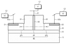
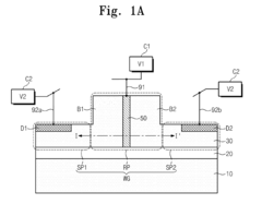
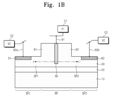
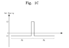
Electro-optic modulating device
PatentActiveUS20110058764A1
Innovation
- The development of an electro-optic modulating device with a vertical structure optical waveguide configuration, including a rib portion with vertical doping regions and body regions forming PN-junctions or PIN-junctions, which allows for increased effective refractive index variation and reduced optical waveguide loss through optimized doping profiles and interconnection structures.
Manufacturing Processes
The manufacturing processes for silicon photonics in flexible electronic devices present unique challenges and opportunities. Traditional silicon photonics fabrication relies on rigid substrates and high-temperature processes, which are incompatible with flexible electronics. To address this, innovative manufacturing techniques have been developed to integrate silicon photonics with flexible substrates.
One key approach is the transfer printing method, which allows for the fabrication of silicon photonic components on a rigid substrate before transferring them onto a flexible platform. This process involves creating release layers, etching sacrificial materials, and using elastomeric stamps to pick up and place the photonic elements. The transfer printing technique enables the preservation of high-performance silicon photonics while achieving flexibility.
Another significant manufacturing innovation is the development of low-temperature deposition processes for silicon-based materials. Plasma-enhanced chemical vapor deposition (PECVD) and sputtering techniques have been optimized to deposit amorphous silicon and silicon nitride at temperatures compatible with flexible substrates. These processes allow for the direct fabrication of photonic waveguides and other components on flexible materials.
Laser-based manufacturing techniques have also emerged as promising solutions for flexible silicon photonics. Femtosecond laser writing enables the creation of three-dimensional photonic structures directly within flexible polymer substrates. This additive manufacturing approach offers unprecedented design freedom and the ability to create complex optical circuits without the need for traditional lithography.
To achieve precise patterning on flexible substrates, advanced lithography techniques have been adapted. Soft lithography methods, such as microcontact printing and nanoimprint lithography, allow for high-resolution patterning of photonic structures on flexible materials. These techniques overcome the limitations of conventional photolithography on non-planar surfaces.
The integration of silicon photonics with flexible electronics also requires innovative packaging and interconnect solutions. Techniques such as flip-chip bonding and through-silicon vias (TSVs) have been modified to accommodate the mechanical stress and strain experienced by flexible devices. Additionally, the development of stretchable optical interconnects using serpentine waveguide designs enables seamless integration of photonic components in flexible systems.
As manufacturing processes continue to evolve, scalability and yield improvement remain critical challenges. Researchers are exploring roll-to-roll fabrication techniques to enable high-throughput production of flexible silicon photonic devices. This approach promises to significantly reduce manufacturing costs and accelerate the commercialization of flexible photonic technologies.
Performance Metrics
Performance metrics play a crucial role in evaluating the effectiveness and potential of silicon photonics innovations for flexible electronic devices. These metrics provide quantitative measures to assess the performance, efficiency, and reliability of photonic components and systems integrated into flexible platforms.
One of the primary performance metrics for silicon photonics in flexible electronics is optical transmission efficiency. This metric measures the ability of photonic components to transmit light signals with minimal loss across flexible substrates. Researchers aim to achieve high transmission efficiency, typically above 90%, to ensure reliable data transfer and signal integrity in flexible devices.
Bandwidth is another critical metric, indicating the range of frequencies or wavelengths that can be effectively transmitted through the photonic system. For flexible electronic applications, a wide bandwidth is desirable to support high-speed data transmission and multi-channel operations. Current state-of-the-art silicon photonics systems on flexible substrates can achieve bandwidths in the range of several tens of gigahertz.
Power consumption is a key consideration for flexible electronic devices, where energy efficiency is paramount. Silicon photonic components integrated into flexible platforms should demonstrate low power consumption, typically measured in milliwatts or microwatts, to extend battery life and reduce heat generation in wearable or portable devices.
Flexibility and durability are unique performance metrics specific to flexible electronic applications. These metrics assess the ability of silicon photonic components to maintain their optical and electrical properties under various bending and stretching conditions. Researchers evaluate the performance degradation of photonic elements when subjected to different bending radii and repeated flexing cycles.
Integration density is another important metric, measuring the number of photonic components that can be packed into a given area of flexible substrate. Higher integration density allows for more complex photonic circuits and increased functionality within compact flexible devices. Current research aims to achieve integration densities comparable to those of rigid silicon photonics platforms.
Thermal stability is crucial for maintaining consistent performance in flexible electronic devices exposed to varying environmental conditions. This metric evaluates how well silicon photonic components maintain their optical properties and performance across a range of temperatures, typically from -20°C to 85°C for consumer electronics applications.
Finally, reliability and longevity metrics assess the long-term performance and durability of silicon photonic components in flexible electronic devices. These metrics include factors such as device lifetime, resistance to environmental factors (e.g., humidity, UV exposure), and performance consistency over extended periods of use.
Unlock deeper insights with Patsnap Eureka Quick Research — get a full tech report to explore trends and direct your research. Try now!
Generate Your Research Report Instantly with AI Agent
Supercharge your innovation with Patsnap Eureka AI Agent Platform!