How silicon photonics facilitates rapid prototyping technologies.
JUL 17, 20259 MIN READ
Generate Your Research Report Instantly with AI Agent
PatSnap Eureka helps you evaluate technical feasibility & market potential.
Silicon Photonics Evolution and Objectives
Silicon photonics has emerged as a transformative technology in the field of integrated optics, revolutionizing the way we approach rapid prototyping in various industries. The evolution of silicon photonics can be traced back to the late 1980s when researchers first explored the potential of using silicon as a platform for optical devices. Over the past three decades, this technology has undergone significant advancements, driven by the increasing demand for high-speed data transmission and processing in telecommunications and computing.
The primary objective of silicon photonics in the context of rapid prototyping is to leverage the well-established semiconductor manufacturing infrastructure to create highly integrated optical circuits. This approach aims to combine the benefits of optical communication with the scalability and cost-effectiveness of silicon-based fabrication processes. By doing so, silicon photonics facilitates the development of compact, energy-efficient, and high-performance photonic devices that can be rapidly prototyped and integrated into various systems.
One of the key drivers behind the evolution of silicon photonics is the need for faster and more efficient data transfer in data centers and high-performance computing environments. As traditional electronic interconnects approach their physical limits, silicon photonics offers a promising solution by enabling optical communication at the chip level. This technology allows for the integration of optical components such as modulators, detectors, and waveguides directly onto silicon chips, paving the way for novel rapid prototyping techniques in the semiconductor industry.
The objectives of silicon photonics in rapid prototyping extend beyond just improving data transmission speeds. Researchers and engineers are also focusing on developing new manufacturing techniques that allow for quick iteration and testing of photonic designs. This includes the use of advanced lithography processes, 3D printing technologies, and novel materials to create complex photonic structures with unprecedented precision and speed.
Furthermore, silicon photonics aims to address the challenges of power consumption and heat dissipation in modern electronic devices. By replacing electrical interconnects with optical ones, silicon photonics can significantly reduce energy consumption while increasing data transfer rates. This aligns with the broader goals of sustainable technology development and green computing initiatives.
As silicon photonics continues to evolve, its impact on rapid prototyping technologies is expected to grow exponentially. The integration of artificial intelligence and machine learning algorithms in the design and optimization of photonic circuits is opening up new possibilities for automated and efficient prototyping processes. Additionally, the development of hybrid photonic-electronic systems is pushing the boundaries of what is possible in terms of device performance and functionality, further accelerating the pace of innovation in rapid prototyping technologies.
Rapid Prototyping Market Analysis
The rapid prototyping market has experienced significant growth in recent years, driven by increasing demand for faster product development cycles and customized manufacturing solutions. This market encompasses various technologies, including 3D printing, CNC machining, and injection molding, with silicon photonics emerging as a promising enabler for advanced rapid prototyping applications.
The global rapid prototyping market was valued at approximately $2.5 billion in 2020 and is projected to reach $8.7 billion by 2027, growing at a CAGR of around 20% during the forecast period. This growth is fueled by the adoption of rapid prototyping technologies across diverse industries such as automotive, aerospace, healthcare, and consumer electronics.
Silicon photonics, a technology that integrates optical components and electronic circuits on silicon chips, is poised to revolutionize the rapid prototyping landscape. By enabling high-speed data transmission and processing, silicon photonics facilitates more efficient and precise prototyping processes. This technology is particularly valuable in industries requiring complex, high-performance prototypes, such as telecommunications and data centers.
The market for silicon photonics in rapid prototyping is still in its early stages but shows promising growth potential. As of 2021, the global silicon photonics market was valued at $1.1 billion, with a projected CAGR of 23.4% from 2022 to 2030. While not all of this market is directly related to rapid prototyping, the technology's applications in this field are expected to contribute significantly to its growth.
Key drivers for the adoption of silicon photonics in rapid prototyping include the increasing demand for high-speed data transmission, the need for energy-efficient solutions, and the push for miniaturization in various industries. The technology's ability to integrate multiple functions on a single chip aligns well with the rapid prototyping market's requirements for speed, precision, and cost-effectiveness.
However, challenges such as high initial investment costs and the need for specialized expertise may slow the widespread adoption of silicon photonics in rapid prototyping. Despite these obstacles, the technology's potential to enhance prototyping capabilities and reduce time-to-market for complex products is expected to drive its integration into rapid prototyping workflows over the coming years.
As the rapid prototyping market continues to evolve, silicon photonics is likely to play an increasingly important role in enabling more sophisticated and efficient prototyping processes. This synergy between silicon photonics and rapid prototyping technologies is expected to create new opportunities for innovation and market growth in the coming decade.
Silicon Photonics: Current State and Challenges
Silicon photonics has emerged as a transformative technology in the field of integrated optics, offering unprecedented opportunities for rapid prototyping and innovation. However, the current state of silicon photonics presents both significant advancements and notable challenges that must be addressed to fully realize its potential in facilitating rapid prototyping technologies.
One of the primary advantages of silicon photonics is its compatibility with existing CMOS fabrication processes, allowing for seamless integration with electronic components. This compatibility has led to the development of high-performance, low-cost photonic integrated circuits (PICs) that can be rapidly prototyped and manufactured at scale. The ability to leverage established semiconductor manufacturing infrastructure has accelerated the adoption of silicon photonics across various industries.
Despite these advancements, silicon photonics faces several technical challenges that hinder its widespread implementation in rapid prototyping scenarios. One significant obstacle is the inherent material limitations of silicon, particularly its indirect bandgap, which makes it inefficient for light emission. This limitation has necessitated the development of hybrid integration approaches, combining silicon with other materials such as III-V semiconductors to achieve efficient light sources.
Another challenge lies in the precise control of optical properties at the nanoscale level. The high refractive index contrast in silicon-based waveguides leads to increased sensitivity to fabrication imperfections, making it difficult to achieve consistent performance across different prototypes. This issue is particularly pronounced in rapid prototyping scenarios, where quick iterations and modifications are essential.
The integration of active components, such as modulators and detectors, presents additional hurdles. While significant progress has been made in developing high-speed silicon-based modulators, achieving efficient, low-power operation remains a challenge. Similarly, the development of high-performance photodetectors integrated directly on silicon substrates continues to be an area of active research.
Thermal management is another critical concern in silicon photonic devices, especially in high-density integration scenarios. The thermo-optic effect in silicon can lead to performance variations and wavelength shifts, necessitating precise temperature control mechanisms. This challenge becomes more pronounced in rapid prototyping environments, where thermal considerations may not be fully addressed in early design iterations.
Despite these challenges, ongoing research and development efforts are continuously pushing the boundaries of silicon photonics technology. Advanced fabrication techniques, such as 3D integration and wafer-scale bonding, are enabling more complex and efficient photonic architectures. Additionally, the development of new materials and hybrid integration approaches is expanding the capabilities of silicon photonics, addressing some of its inherent limitations.
Silicon Photonics in Rapid Prototyping: Solutions
01 Rapid prototyping techniques for silicon photonics
Various rapid prototyping techniques are employed in silicon photonics to accelerate the development and testing of photonic devices. These methods include 3D printing, laser-based fabrication, and other additive manufacturing processes that allow for quick iteration and optimization of photonic components.- Rapid prototyping techniques for silicon photonics: Various rapid prototyping techniques are employed in silicon photonics to accelerate the development and testing of photonic devices. These methods include 3D printing, laser-based fabrication, and other additive manufacturing processes that allow for quick iteration and optimization of photonic components.
- Integration of silicon photonics with existing manufacturing processes: Efforts are made to integrate silicon photonics fabrication with established semiconductor manufacturing processes. This integration enables the use of existing infrastructure and expertise, facilitating faster prototyping and production of photonic devices alongside electronic components.
- Novel materials and structures for silicon photonics: Research focuses on developing new materials and structures to enhance the performance of silicon photonic devices. This includes the exploration of hybrid materials, nanostructures, and novel geometries that can be rapidly prototyped and tested for improved optical properties and functionality.
- Automated design and simulation tools for silicon photonics: Advanced software tools are developed for the automated design and simulation of silicon photonic devices. These tools enable rapid virtual prototyping, optimization, and testing of photonic circuits before physical fabrication, significantly reducing development time and costs.
- Packaging and testing solutions for rapid prototyping: Innovative packaging and testing solutions are created to support the rapid prototyping of silicon photonic devices. These include modular packaging approaches, automated testing systems, and standardized interfaces that allow for quick assembly and characterization of photonic prototypes.
02 Integration of silicon photonics with existing manufacturing processes
Efforts are made to integrate silicon photonics fabrication with existing semiconductor manufacturing processes. This integration allows for more efficient production and easier adoption of silicon photonics technology in various applications, including data centers and telecommunications.Expand Specific Solutions03 Novel materials and structures for silicon photonics
Research focuses on developing new materials and structures to enhance the performance of silicon photonic devices. This includes the exploration of hybrid materials, metamaterials, and nanostructures to improve light manipulation and transmission in photonic circuits.Expand Specific Solutions04 Automated design and optimization tools for silicon photonics
Advanced software tools and algorithms are developed to automate the design and optimization of silicon photonic components and circuits. These tools enable rapid iteration and testing of designs, reducing development time and improving overall performance.Expand Specific Solutions05 Testing and characterization methods for rapid prototyping
Innovative testing and characterization techniques are developed to quickly assess the performance of silicon photonic prototypes. These methods include on-chip testing, high-speed measurement systems, and automated quality control processes to ensure rapid iteration and validation of designs.Expand Specific Solutions
Key Players in Silicon Photonics Industry
The silicon photonics industry is in a growth phase, with rapid advancements in technology and increasing market adoption. The global market for silicon photonics is projected to expand significantly in the coming years, driven by demand for high-speed data transmission and energy-efficient computing solutions. Key players like Intel, IBM, and Huawei are investing heavily in research and development, while specialized companies such as Skorpios Technologies and Advanced Micro Foundry are pushing the boundaries of innovation. Academic institutions like MIT and Nanyang Technological University are also contributing to technological advancements. The technology's maturity is progressing, with companies like TSMC and Applied Materials working on manufacturing processes to enable large-scale production and commercialization of silicon photonic devices.
Taiwan Semiconductor Manufacturing Co., Ltd.
Technical Solution: TSMC's silicon photonics technology enables rapid prototyping through its advanced foundry services and integrated design ecosystem. The company offers a comprehensive silicon photonics platform that includes a wide range of passive and active photonic components[8]. TSMC's process design kits (PDKs) for silicon photonics provide designers with accurate models and tools for rapid simulation and optimization of photonic circuits. The company's multi-project wafer (MPW) services allow for cost-effective prototyping of small-volume designs, enabling quick iteration and testing[9]. TSMC's silicon photonics technology supports high-speed optical interconnects, with data rates exceeding 100 Gbps per channel, facilitating rapid prototyping of next-generation communication systems[10].
Strengths: Advanced foundry capabilities, comprehensive design ecosystem, cost-effective MPW services. Weaknesses: Potential capacity constraints due to high demand across various semiconductor technologies.
Huawei Technologies Co., Ltd.
Technical Solution: Huawei's approach to silicon photonics for rapid prototyping focuses on developing a flexible and scalable platform. The company has invested in advanced photonic integration techniques that allow for quick design and fabrication of complex photonic circuits[5]. Huawei's silicon photonics technology supports a wide range of applications, from data centers to 5G networks, enabling rapid prototyping across various domains. The company has developed a library of standardized photonic components that can be easily combined to create custom designs, significantly reducing development time[6]. Huawei's silicon photonics platform incorporates advanced packaging technologies, such as 2.5D and 3D integration, which facilitate the rapid prototyping of hybrid electro-optical systems[7].
Strengths: Versatile platform supporting multiple applications, extensive library of standardized components. Weaknesses: Potential geopolitical challenges affecting global collaboration and market access.
Core Innovations in Silicon Photonics
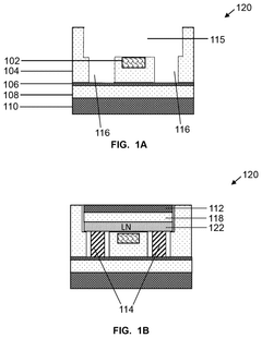
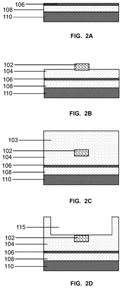
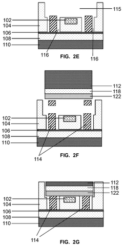
A hybrid silicon photonics modulator and method to manufacture the same
PatentPendingUS20250164829A1
Innovation
- A hybrid silicon photonics modulator is developed by bonding a CMOS-compatible SOI wafer with a non-CMOS compatible LNOI wafer via electrodes and/or a lithium niobate layer, ensuring compatibility with both lithium-niobate and silicon devices.
Integration Challenges and Opportunities
The integration of silicon photonics with rapid prototyping technologies presents both significant challenges and exciting opportunities. One of the primary challenges lies in the precise alignment and coupling of optical components at the nanoscale level. This requires advanced fabrication techniques and sophisticated equipment, which can be costly and time-consuming to implement in a rapid prototyping environment.
Another challenge is the thermal management of integrated photonic circuits. As these circuits become more complex and densely packed, heat dissipation becomes a critical issue that can affect the performance and reliability of the devices. Developing effective cooling solutions that are compatible with rapid prototyping processes is essential for the successful integration of silicon photonics.
The integration of electronic and photonic components on a single chip also poses challenges in terms of material compatibility and process integration. Rapid prototyping technologies must be adapted to handle both electronic and photonic elements, which often have different fabrication requirements and tolerances.
Despite these challenges, the integration of silicon photonics with rapid prototyping technologies offers numerous opportunities. One of the most promising is the potential for faster design iterations and reduced time-to-market for photonic devices. By leveraging rapid prototyping techniques, researchers and engineers can quickly test and refine their designs, accelerating the development cycle of photonic systems.
The integration also opens up possibilities for novel hybrid devices that combine the best features of both electronic and photonic technologies. This could lead to the creation of more efficient and compact systems for applications in telecommunications, data centers, and sensing.
Furthermore, the convergence of silicon photonics and rapid prototyping could democratize access to photonic technology. As fabrication processes become more accessible and cost-effective, smaller companies and research institutions may be able to participate more actively in photonics innovation, potentially leading to a broader range of applications and breakthroughs in the field.
Addressing these integration challenges will require collaborative efforts between experts in silicon photonics, rapid prototyping, materials science, and thermal management. As solutions are developed, they will likely drive advancements in both fields, leading to more sophisticated and versatile rapid prototyping technologies that can handle the complexities of photonic systems.
Economic Impact of Silicon Photonics Prototyping
The economic impact of silicon photonics prototyping is significant and far-reaching, affecting various sectors of the technology industry and beyond. As silicon photonics enables rapid prototyping technologies, it accelerates innovation cycles and reduces time-to-market for new products. This acceleration has a ripple effect throughout the supply chain, stimulating economic growth and job creation in related industries.
One of the primary economic benefits of silicon photonics prototyping is the substantial reduction in development costs. Traditional prototyping methods often require expensive equipment and materials, whereas silicon photonics leverages existing semiconductor manufacturing infrastructure. This cost-effectiveness allows smaller companies and startups to enter the market, fostering a more competitive and innovative ecosystem.
The rapid prototyping capabilities of silicon photonics also lead to increased productivity in research and development departments. Engineers and scientists can iterate designs more quickly, leading to faster breakthroughs and more efficient use of resources. This enhanced productivity translates into higher returns on investment for companies engaged in photonics-related research and development.
Furthermore, the integration of silicon photonics in prototyping processes has spurred the growth of specialized job markets. As demand for expertise in this field increases, universities and training programs have expanded their offerings, creating a skilled workforce that supports the burgeoning industry. This talent pool becomes a valuable economic asset, attracting investment and fostering regional technology hubs.
The economic impact extends to adjacent industries as well. As silicon photonics enables more efficient and powerful optical communication systems, it drives advancements in data centers, telecommunications, and cloud computing. These improvements in digital infrastructure have wide-ranging economic benefits, enhancing productivity across various sectors and enabling new business models in the digital economy.
Moreover, the rapid prototyping capabilities facilitated by silicon photonics contribute to the development of cutting-edge technologies in fields such as autonomous vehicles, augmented reality, and medical imaging. These innovations not only create new market opportunities but also have the potential to solve complex societal challenges, further amplifying their economic impact.
In conclusion, the economic ramifications of silicon photonics prototyping are multifaceted and substantial. By accelerating innovation, reducing costs, increasing productivity, and enabling new technologies, it serves as a catalyst for economic growth and technological advancement across multiple industries.
Unlock deeper insights with PatSnap Eureka Quick Research — get a full tech report to explore trends and direct your research. Try now!
Generate Your Research Report Instantly with AI Agent
Supercharge your innovation with PatSnap Eureka AI Agent Platform!