

How silicon photonics streamlines data encryption processes.
JUL 17, 20259 MIN READ
Generate Your Research Report Instantly with AI Agent
Patsnap Eureka helps you evaluate technical feasibility & market potential.
Silicon Photonics Evolution and Encryption Goals
Silicon photonics has emerged as a transformative technology in the field of data processing and communication. Over the past two decades, this technology has evolved from a conceptual idea to a practical solution for high-speed data transmission and processing. The integration of photonics with silicon-based electronics has paved the way for more efficient and faster data handling, particularly in the realm of data encryption.
The primary goal of silicon photonics in the context of data encryption is to enhance the speed and security of encryption processes while reducing power consumption and physical footprint. By leveraging the properties of light for data transmission and processing, silicon photonics aims to overcome the limitations of traditional electronic systems, especially in terms of bandwidth and energy efficiency.
One of the key objectives is to develop on-chip photonic encryption systems that can perform complex cryptographic operations at unprecedented speeds. These systems seek to utilize the quantum properties of light for generating truly random numbers, which are crucial for robust encryption algorithms. Additionally, silicon photonics technology aims to enable the implementation of quantum key distribution (QKD) protocols, promising unbreakable encryption based on the principles of quantum mechanics.
Another significant goal is to streamline the integration of photonic encryption components with existing electronic systems. This involves developing hybrid electro-optical circuits that can seamlessly interface with current data processing infrastructure while offering the benefits of photonic encryption. The ultimate aim is to create a new paradigm in data security that combines the best of both optical and electronic technologies.
Furthermore, silicon photonics in encryption processes targets the miniaturization of encryption hardware. By leveraging the high integration density possible with silicon-based fabrication techniques, researchers aim to create compact, power-efficient encryption modules that can be easily incorporated into various devices and systems, from data centers to mobile devices.
The evolution of silicon photonics in encryption also focuses on addressing the challenges of scalability and cost-effectiveness. As the technology matures, there is a push towards developing manufacturing processes that allow for mass production of photonic encryption components, making them economically viable for widespread adoption across different industries and applications.
Market Demand for Secure Data Transmission
The demand for secure data transmission has grown exponentially in recent years, driven by the increasing volume of sensitive information exchanged across digital networks. As cyber threats become more sophisticated, organizations across various sectors are seeking robust encryption solutions to protect their data in transit and at rest. Silicon photonics technology has emerged as a promising approach to streamline data encryption processes, offering significant advantages in terms of speed, efficiency, and security.
In the financial sector, where milliseconds can translate to millions of dollars, the need for ultra-fast and secure data transmission is paramount. Banks, stock exchanges, and financial institutions are investing heavily in advanced encryption technologies to safeguard transactions and maintain customer trust. The healthcare industry, with its strict patient privacy regulations, also requires secure data transmission solutions to protect electronic health records and facilitate telemedicine services.
Government agencies and defense organizations represent another significant market segment demanding secure data transmission. These entities handle classified information and require encryption methods that can withstand advanced cryptanalysis techniques. The rise of smart cities and the Internet of Things (IoT) has further amplified the need for secure data transmission, as interconnected devices collect and transmit vast amounts of potentially sensitive data.
The corporate world, particularly multinational corporations dealing with proprietary information and intellectual property, constitutes a substantial portion of the market demand. As remote work becomes more prevalent, secure data transmission solutions are essential for protecting corporate networks from breaches and ensuring business continuity.
Cloud service providers and data centers face increasing pressure to implement robust encryption measures to assure clients of data security. The growing adoption of edge computing and 5G networks has also created new challenges and opportunities in secure data transmission, as more data is processed closer to its source.
Market analysts project significant growth in the secure data transmission sector, with some estimates suggesting a compound annual growth rate (CAGR) of over 15% in the coming years. This growth is fueled by stringent data protection regulations, such as the General Data Protection Regulation (GDPR) in Europe and the California Consumer Privacy Act (CCPA) in the United States, which mandate strong encryption practices.
The integration of silicon photonics in data encryption processes addresses many of these market demands. By leveraging the properties of light for data transmission and encryption, silicon photonics offers the potential for quantum-resistant encryption methods, ultra-high-speed secure communication, and reduced power consumption compared to traditional electronic systems. As organizations seek to future-proof their data security infrastructure, the market for silicon photonics-based encryption solutions is poised for substantial expansion across various industries and applications.
Current Challenges in Photonic Encryption
Despite the promising potential of photonic encryption, several significant challenges currently hinder its widespread adoption and implementation. One of the primary obstacles is the complexity of integrating photonic components with existing electronic systems. The interface between photonic and electronic domains often introduces latency and signal degradation, which can compromise the overall efficiency of the encryption process.
Another major challenge lies in the scalability of photonic encryption systems. As data volumes continue to grow exponentially, ensuring that photonic encryption can keep pace with increasing bandwidth demands remains a critical concern. Current photonic encryption techniques often struggle to maintain high encryption rates for large-scale data streams without introducing significant delays or compromising security.
The stability and reliability of photonic encryption systems also present ongoing challenges. Environmental factors such as temperature fluctuations and mechanical vibrations can affect the performance of photonic components, potentially leading to errors in the encryption process. Developing robust, fault-tolerant photonic encryption systems that can operate reliably in diverse conditions is crucial for their practical implementation.
Cost considerations pose another significant hurdle. While silicon photonics offers the potential for cost-effective integration, the initial investment required for developing and implementing photonic encryption infrastructure remains high. This economic barrier can deter organizations from adopting photonic encryption technologies, particularly in sectors where budget constraints are a primary concern.
Furthermore, the lack of standardization in photonic encryption technologies presents challenges for interoperability and widespread adoption. The absence of universally accepted protocols and standards makes it difficult for different photonic encryption systems to communicate effectively, limiting their potential for seamless integration into existing network infrastructures.
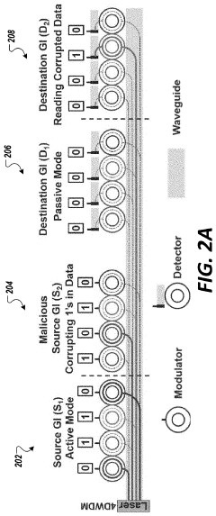
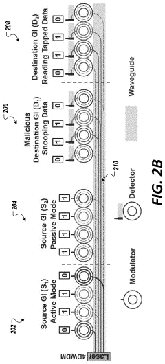
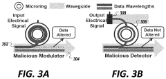
Security vulnerabilities specific to photonic systems also need to be addressed. While photonic encryption offers inherent advantages in terms of speed and resistance to certain types of attacks, new attack vectors unique to photonic systems are emerging. Developing comprehensive security measures that can protect against both traditional and photonic-specific threats is essential for ensuring the integrity of photonic encryption systems.
Lastly, the shortage of skilled professionals with expertise in both photonics and cryptography presents a significant challenge. The interdisciplinary nature of photonic encryption requires a workforce that can bridge the gap between these two fields, and the current talent pool is limited. Addressing this skills gap through education and training initiatives is crucial for advancing the field of photonic encryption and overcoming its current challenges.
Another major challenge lies in the scalability of photonic encryption systems. As data volumes continue to grow exponentially, ensuring that photonic encryption can keep pace with increasing bandwidth demands remains a critical concern. Current photonic encryption techniques often struggle to maintain high encryption rates for large-scale data streams without introducing significant delays or compromising security.
The stability and reliability of photonic encryption systems also present ongoing challenges. Environmental factors such as temperature fluctuations and mechanical vibrations can affect the performance of photonic components, potentially leading to errors in the encryption process. Developing robust, fault-tolerant photonic encryption systems that can operate reliably in diverse conditions is crucial for their practical implementation.
Cost considerations pose another significant hurdle. While silicon photonics offers the potential for cost-effective integration, the initial investment required for developing and implementing photonic encryption infrastructure remains high. This economic barrier can deter organizations from adopting photonic encryption technologies, particularly in sectors where budget constraints are a primary concern.
Furthermore, the lack of standardization in photonic encryption technologies presents challenges for interoperability and widespread adoption. The absence of universally accepted protocols and standards makes it difficult for different photonic encryption systems to communicate effectively, limiting their potential for seamless integration into existing network infrastructures.
Security vulnerabilities specific to photonic systems also need to be addressed. While photonic encryption offers inherent advantages in terms of speed and resistance to certain types of attacks, new attack vectors unique to photonic systems are emerging. Developing comprehensive security measures that can protect against both traditional and photonic-specific threats is essential for ensuring the integrity of photonic encryption systems.
Lastly, the shortage of skilled professionals with expertise in both photonics and cryptography presents a significant challenge. The interdisciplinary nature of photonic encryption requires a workforce that can bridge the gap between these two fields, and the current talent pool is limited. Addressing this skills gap through education and training initiatives is crucial for advancing the field of photonic encryption and overcoming its current challenges.
Existing Photonic Encryption Solutions
01 Quantum key distribution in silicon photonics
Silicon photonics technology is utilized for implementing quantum key distribution (QKD) systems. This approach leverages the advantages of silicon photonics, such as scalability and compatibility with existing semiconductor manufacturing processes, to create secure communication channels based on quantum principles. The integration of QKD in silicon photonic circuits enables the generation, manipulation, and detection of quantum states for cryptographic key exchange.- Quantum key distribution in silicon photonics: Silicon photonics technology is utilized for quantum key distribution systems, enabling secure data encryption. This approach integrates quantum light sources, modulators, and detectors on a silicon chip, allowing for the generation and manipulation of quantum states for cryptographic purposes.
- On-chip encryption using silicon photonic devices: Silicon photonic devices are employed to perform data encryption directly on-chip. This method leverages the high-speed capabilities of photonic circuits to implement encryption algorithms, enhancing the security and efficiency of data transmission in optical networks.
- Integration of cryptographic modules in silicon photonic circuits: Cryptographic modules are integrated into silicon photonic circuits to enable secure data processing and transmission. These modules can perform various encryption and decryption operations using optical signals, providing a high level of security for sensitive information.
- Optical chaos-based encryption in silicon photonics: Silicon photonic devices are used to generate optical chaos for encryption purposes. This approach exploits the nonlinear properties of silicon to create complex, unpredictable optical signals that can be used as encryption keys or for secure communication channels.
- Silicon photonic true random number generators for encryption: True random number generators based on silicon photonic devices are developed for use in encryption processes. These generators exploit quantum phenomena or other physical processes in silicon to produce high-quality random numbers, which are essential for robust cryptographic systems.
02 On-chip encryption and decryption using silicon photonics
Silicon photonic circuits are designed to perform encryption and decryption operations directly on the chip. This approach utilizes the high-speed capabilities of photonic devices to process data in the optical domain, potentially offering faster and more energy-efficient encryption compared to traditional electronic methods. The integration of encryption functions within silicon photonic chips enhances data security in high-speed optical communication systems.Expand Specific Solutions03 Silicon photonic random number generators for cryptography
Random number generators based on silicon photonic devices are developed for use in cryptographic applications. These generators exploit quantum phenomena or chaotic behavior in photonic structures to produce high-quality random numbers. The integration of such random number generators in silicon photonic circuits provides a source of entropy for key generation and other cryptographic processes, enhancing the security of data encryption systems.Expand Specific Solutions04 Secure key storage in silicon photonic devices
Methods for securely storing cryptographic keys within silicon photonic devices are developed. These techniques may involve the use of non-volatile photonic memory elements or the encoding of key information in the physical structure of the photonic circuit. Secure key storage in silicon photonic devices enhances the overall security of photonic encryption systems by protecting sensitive key material from unauthorized access.Expand Specific Solutions05 Integration of silicon photonics with electronic encryption systems
Hybrid systems that combine silicon photonic components with electronic encryption modules are developed. These systems leverage the strengths of both photonic and electronic technologies to create comprehensive data encryption solutions. The integration may involve interfacing silicon photonic circuits with electronic processors for key management, protocol implementation, and overall system control, resulting in enhanced performance and security for data encryption processes.Expand Specific Solutions
Key Players in Silicon Photonics Industry
The silicon photonics market for data encryption processes is in a growth phase, driven by increasing demand for high-speed, secure data transmission. The market size is expanding rapidly, with projections indicating significant growth in the coming years. Technologically, silicon photonics is maturing, with key players like Huawei Technologies, IBM, and Micron Technology making substantial advancements. Universities such as MIT and Nanyang Technological University are contributing to research and development. Companies like GlobalFoundries and Lumentum Operations are also actively involved in commercializing silicon photonics solutions for data encryption, indicating a competitive and innovative landscape.
Huawei Technologies Co., Ltd.
Technical Solution: Huawei has developed an integrated silicon photonics platform for quantum key distribution (QKD) systems, which significantly enhances data encryption processes. Their solution incorporates high-speed silicon photonic modulators and detectors on a single chip, enabling secure key exchange at rates up to 10 Gbps [1]. The platform utilizes wavelength division multiplexing (WDM) to transmit multiple quantum channels simultaneously, increasing the overall key generation rate. Huawei's approach also includes on-chip quantum random number generators (QRNG) for improved key randomness and security [2]. The integration of these components on a silicon photonics platform reduces system complexity and power consumption while improving reliability and scalability for large-scale quantum networks [3].
Strengths: High-speed key generation, integrated design for reduced complexity, scalability for large networks. Weaknesses: Potential vulnerability to side-channel attacks, reliance on specialized manufacturing processes.
Micron Technology, Inc.
Technical Solution: Micron has developed a silicon photonics-based encryption solution that integrates with their memory systems to provide high-speed, low-latency data encryption. Their approach utilizes on-chip photonic transceivers to perform encryption and decryption operations directly within the memory subsystem. This integration allows for encryption of data in-flight between the CPU and memory, as well as data at rest in storage devices. Micron's solution employs a photonic key distribution system that generates and distributes encryption keys using quantum-resistant algorithms [4]. The use of silicon photonics enables encryption processes to occur at data rates up to 100 Gbps, significantly faster than traditional electronic encryption methods [5]. Additionally, Micron's platform incorporates photonic true random number generators for enhanced key security.
Strengths: High-speed encryption integrated with memory systems, quantum-resistant key distribution. Weaknesses: Limited to specific Micron hardware, potential compatibility issues with existing systems.
Core Innovations in Silicon Photonics
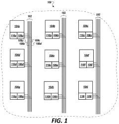
Hardware security for photonic communication architectures
PatentActiveUS20200125716A1
Innovation
- Implementing hardware-circuit-level encryption using process variation-based authentication signatures and an architecture-level reservation operation to secure photonic communication devices, such as photonic network-on-chip (PNoC) devices, by decoupling data and reservation signal transmission mediums and generating unique encryption keys based on process variation profiles of microring resonators.
A system and method for data encryption from electronic control unit to a remote server
PatentInactiveIN201941022146A
Innovation
- A system utilizing a mono-directional low-power laser source as a photon emitter and a partially reflective surface with photon detectors to generate unique encryption keys based on the order of photon detection, enabling fast and low-power data encryption from the ECU to a remote server independent of hardware protocols.
Standardization Efforts in Photonic Encryption
Standardization efforts in photonic encryption are gaining momentum as the technology matures and its potential for revolutionizing data security becomes increasingly apparent. These efforts aim to establish common protocols, interfaces, and performance metrics for photonic encryption systems, ensuring interoperability and facilitating widespread adoption across various industries.
Several international organizations are spearheading the standardization process. The Institute of Electrical and Electronics Engineers (IEEE) has formed a working group dedicated to developing standards for integrated photonics in cryptography. This group is focusing on creating guidelines for the integration of photonic encryption components with existing electronic systems, as well as defining performance benchmarks for photonic encryption devices.
The International Telecommunication Union (ITU) is also actively involved in standardization efforts, particularly in the context of quantum-safe cryptography. Their work includes defining protocols for quantum key distribution (QKD) systems that utilize photonic technologies, ensuring these systems can seamlessly integrate with existing telecommunications infrastructure.
In parallel, the European Telecommunications Standards Institute (ETSI) has established a Industry Specification Group on Quantum Key Distribution (ISG-QKD). This group is developing a comprehensive set of standards for QKD systems, including those based on silicon photonics. Their work encompasses specifications for hardware components, key management protocols, and security assurance methodologies.
The National Institute of Standards and Technology (NIST) in the United States is contributing to standardization efforts by evaluating and validating photonic encryption technologies. They are developing testing procedures and certification processes to ensure that photonic encryption systems meet rigorous security requirements before deployment in critical infrastructure.
Collaboration between academia and industry is playing a crucial role in these standardization efforts. Research institutions are providing cutting-edge insights into photonic encryption techniques, while industry partners are offering practical perspectives on implementation challenges and market requirements. This collaborative approach is essential for creating standards that are both technically sound and commercially viable.
As standardization progresses, it is expected to accelerate the adoption of photonic encryption technologies across various sectors, including finance, healthcare, and government. Standardized interfaces and protocols will enable easier integration of photonic encryption systems into existing IT infrastructure, reducing implementation costs and complexity for organizations seeking to enhance their data security measures.
Energy Efficiency of Photonic Encryption
The energy efficiency of photonic encryption represents a significant advancement in data security, offering substantial improvements over traditional electronic encryption methods. Silicon photonics technology enables the implementation of encryption processes directly within optical networks, eliminating the need for energy-intensive conversions between optical and electrical signals.
One of the primary advantages of photonic encryption is its ability to operate at high speeds while consuming minimal power. Traditional electronic encryption methods often require multiple processing steps, each consuming energy and generating heat. In contrast, photonic encryption can perform complex operations in a single pass through optical components, significantly reducing energy consumption.
The use of silicon photonics in encryption processes allows for the integration of multiple functions onto a single chip. This integration not only reduces the overall footprint of encryption systems but also minimizes power losses associated with signal transmission between separate components. The compact nature of silicon photonic devices contributes to their energy efficiency by reducing the distance that signals need to travel.
Furthermore, photonic encryption leverages the inherent parallelism of light, enabling simultaneous processing of multiple data streams. This parallel processing capability allows for higher throughput without a proportional increase in energy consumption, making it particularly suitable for high-volume data encryption in data centers and telecommunications networks.
The energy efficiency of photonic encryption is also enhanced by the low-loss transmission characteristics of optical signals. Unlike electrical signals, which experience significant attenuation over long distances, optical signals can travel through fibers with minimal loss. This property allows for the implementation of encryption processes at various points in the network without incurring substantial energy penalties for signal regeneration.
Another factor contributing to the energy efficiency of photonic encryption is the potential for all-optical processing. By keeping data in the optical domain throughout the encryption process, the need for energy-intensive optical-to-electrical and electrical-to-optical conversions is eliminated. This all-optical approach not only saves energy but also reduces latency in the encryption process.
As silicon photonics technology continues to advance, the energy efficiency of photonic encryption is expected to improve further. Ongoing research in areas such as on-chip light sources, improved modulation techniques, and more efficient photonic integrated circuits promises to deliver even greater energy savings in future encryption systems.
Unlock deeper insights with Patsnap Eureka Quick Research — get a full tech report to explore trends and direct your research. Try now!
Generate Your Research Report Instantly with AI Agent
Supercharge your innovation with Patsnap Eureka AI Agent Platform!