

How to Evaluate OLED Electroluminescent Layer Uniformity
SEP 12, 20259 MIN READ
Generate Your Research Report Instantly with AI Agent
PatSnap Eureka helps you evaluate technical feasibility & market potential.
OLED Uniformity Evaluation Background and Objectives
Organic Light-Emitting Diode (OLED) technology has revolutionized display and lighting industries since its commercial introduction in the late 1990s. The evolution of OLED technology has been marked by significant improvements in efficiency, lifetime, and manufacturing processes. The electroluminescent layer, where light emission occurs through recombination of electrons and holes, represents the core functional component of any OLED device. The uniformity of this layer directly impacts display quality, energy efficiency, and device longevity.
Historical developments in OLED uniformity evaluation began with simple visual inspection methods, progressing through various optical measurement techniques to today's sophisticated analytical instruments. Early challenges in achieving uniform electroluminescent layers stemmed from limitations in deposition technologies, particularly for large-area displays. The industry has witnessed a gradual shift from rudimentary evaluation methods to quantitative assessment protocols that can detect nanoscale variations.
The primary objective of OLED electroluminescent layer uniformity evaluation is to establish standardized, reliable, and reproducible measurement methodologies that can accurately characterize spatial variations in emission properties. These evaluations aim to identify defects, inconsistencies, and performance variations that may compromise the final product quality or manufacturing yield.
Current technical goals include developing high-resolution mapping techniques capable of detecting sub-micron non-uniformities, establishing correlation models between manufacturing parameters and uniformity outcomes, and implementing real-time monitoring systems for production environments. Additionally, there is growing emphasis on creating predictive models that can anticipate uniformity issues before they manifest in finished devices.
The technological trajectory points toward integration of artificial intelligence and machine learning algorithms to enhance detection capabilities and automate evaluation processes. Emerging spectroscopic techniques with higher spatial resolution are being explored to provide more detailed characterization of layer properties beyond simple brightness variations.
Industry standards for uniformity evaluation continue to evolve, with organizations like the International Electrotechnical Commission (IEC) and Society for Information Display (SID) working to establish common metrics and testing protocols. These standardization efforts are crucial for enabling meaningful comparisons between different manufacturing processes and technologies.
As OLED applications expand beyond traditional displays into flexible electronics, transparent displays, and lighting solutions, uniformity evaluation methodologies must adapt to address unique challenges presented by novel form factors and operating conditions. The ultimate goal remains consistent: ensuring pixel-to-pixel consistency that delivers seamless visual experiences and reliable device performance across increasingly diverse applications.
Market Demands for High-Quality OLED Displays
The global OLED display market has witnessed substantial growth, driven primarily by increasing consumer demand for superior visual experiences across various electronic devices. As of 2023, the market valuation exceeds $48 billion, with projections indicating a compound annual growth rate of approximately 14% through 2028. This robust growth trajectory underscores the critical importance of display quality as a key differentiator in consumer electronics.
Consumer expectations for display performance have evolved dramatically, with particular emphasis on color accuracy, brightness uniformity, and overall visual consistency. Market research indicates that over 70% of smartphone users consider display quality among the top three factors influencing their purchasing decisions. This consumer preference has created intense competition among device manufacturers to deliver increasingly refined visual experiences.
The premium segment of the market demonstrates even stronger demand for perfect uniformity in OLED displays. In high-end televisions, professional monitors, and flagship smartphones, even minor inconsistencies in luminance across the display surface can significantly impact consumer satisfaction and brand perception. Industry surveys reveal that visible non-uniformities reduce consumer willingness to pay by up to 25% for otherwise identical products.
Automotive displays represent another rapidly expanding market segment with stringent requirements for OLED uniformity. As vehicles incorporate more sophisticated infotainment systems and digital dashboards, the automotive industry has established exceptionally high standards for display performance under variable lighting conditions. The automotive display market is expected to grow at 17% annually, with OLED technology gaining significant market share due to its superior contrast and form factor flexibility.
Healthcare and medical imaging applications further drive demand for highly uniform OLED displays. Diagnostic accuracy in medical imaging depends critically on display consistency, creating a specialized market segment where performance requirements far exceed consumer-grade specifications. The medical display market, though smaller in volume, commands premium pricing that reflects the critical nature of display performance in clinical settings.
Manufacturing yield improvements represent a significant economic driver for enhanced uniformity evaluation methods. Current industry data suggests that display panel rejection rates due to uniformity issues range from 8% to 15% in mass production. Advanced evaluation techniques that can identify uniformity problems earlier in the production process could potentially reduce these rejection rates by half, translating to billions in manufacturing cost savings across the industry.
Current Challenges in Electroluminescent Layer Uniformity Assessment
The assessment of electroluminescent layer uniformity in OLED displays presents significant technical challenges that impede both manufacturing efficiency and product quality. Current evaluation methods struggle with balancing precision, speed, and cost-effectiveness, creating bottlenecks in production processes. Traditional optical measurement techniques often fail to detect subtle variations in luminance that can significantly impact display performance over time.
One major challenge lies in the multi-scale nature of uniformity defects, which range from microscopic pixel-level inconsistencies to macroscopic regional variations across the display panel. Existing imaging systems typically optimize for either high-resolution microscopic analysis or broad-area scanning, but rarely achieve excellence in both simultaneously. This forces manufacturers to implement multiple testing stages, increasing production time and costs.
Real-time monitoring presents another substantial hurdle. Most current evaluation systems operate as end-of-line testing rather than in-process monitoring, limiting manufacturers' ability to make immediate adjustments during deposition processes. The delay between layer formation and quality assessment results in material waste and reduced yield rates when defects are detected too late in the production cycle.
Environmental sensitivity further complicates uniformity assessment. Electroluminescent layers exhibit different optical properties under varying temperature, humidity, and ambient light conditions. Many evaluation systems fail to account for these environmental factors, leading to inconsistent measurements between laboratory testing and real-world performance.
The correlation between measured physical parameters and actual visual perception represents a fundamental challenge. Instruments may detect variations in thickness or composition that don't necessarily translate to perceptible visual differences, or conversely, miss subtle variations that significantly impact user experience. This disconnect between instrumental measurement and human perception creates uncertainty in defining acceptable uniformity thresholds.
Data interpretation and analysis bottlenecks also persist. Current systems generate massive datasets that require sophisticated algorithms to process effectively. Many manufacturers lack standardized methods for translating raw uniformity data into actionable insights, resulting in subjective decision-making regarding panel acceptance or rejection.
Finally, accelerated aging effects remain difficult to predict from initial uniformity measurements. Current evaluation methods provide limited correlation between initial uniformity characteristics and long-term degradation patterns. This gap in predictive capability forces manufacturers to implement conservative specifications or extensive reliability testing, both of which increase production costs and time-to-market.
Established Methods for Evaluating EL Layer Uniformity
01 Deposition techniques for uniform electroluminescent layers
Various deposition methods can be employed to achieve uniform electroluminescent layers in OLEDs. These include vapor deposition, spin coating, inkjet printing, and other precision application techniques. The uniformity of the electroluminescent layer significantly impacts the device performance, efficiency, and lifetime. Controlling parameters such as temperature, pressure, and deposition rate during the manufacturing process helps ensure consistent layer thickness and composition across the substrate.- Deposition techniques for uniform electroluminescent layers: Various deposition techniques are employed to achieve uniform electroluminescent layers in OLEDs. These include vapor deposition, spin coating, inkjet printing, and other precision application methods that ensure consistent thickness and composition across the substrate. Proper control of these deposition processes is critical for preventing defects and ensuring uniform light emission across the display area.
- Material composition for enhanced layer uniformity: The selection and formulation of materials used in the electroluminescent layer significantly impacts uniformity. Specific organic compounds, host-dopant systems, and polymer blends are designed to promote even distribution during application and prevent aggregation or crystallization. These materials are engineered to maintain consistent morphology throughout the layer, which is essential for uniform light emission and device performance.
- Processing parameters and environmental controls: Controlling processing parameters such as temperature, humidity, and atmospheric conditions during OLED fabrication is crucial for electroluminescent layer uniformity. Precise environmental controls prevent contamination and ensure consistent solvent evaporation rates. Annealing processes and curing conditions are optimized to promote uniform film formation and prevent defects that could lead to non-uniform emission.
- Substrate preparation and interface engineering: Proper preparation of the substrate and engineering of interfaces between layers significantly impacts the uniformity of the electroluminescent layer. Surface treatments, planarization techniques, and buffer layers help create smooth foundations for subsequent layer deposition. These approaches minimize surface energy variations and improve wetting characteristics, leading to more uniform electroluminescent layers and better device performance.
- Quality control and defect management: Advanced quality control methods and defect management strategies are implemented to ensure electroluminescent layer uniformity. These include in-line monitoring systems, optical inspection techniques, and feedback control mechanisms that detect and correct non-uniformities during fabrication. Post-deposition treatments and repair techniques are also employed to address localized defects and improve overall layer uniformity.
02 Material composition for enhanced layer uniformity
The selection and formulation of materials used in the electroluminescent layer significantly affects uniformity. Host materials, dopants, and their ratios must be carefully controlled to prevent aggregation and phase separation. Small molecule and polymer-based materials have different processing requirements for achieving uniform layers. Additives can be incorporated to improve film formation properties, wetting characteristics, and prevent crystallization that would otherwise disrupt layer uniformity.Expand Specific Solutions03 Multi-layer structure optimization for uniformity
Implementing multi-layer structures in the OLED architecture can improve the overall uniformity of the electroluminescent layer. Buffer layers, charge transport layers, and blocking layers help control charge distribution and exciton formation. The interfaces between these layers must be carefully engineered to prevent defects and ensure smooth transitions. Graded compositions or intermediate layers can be used to reduce stress and improve adhesion between different functional layers.Expand Specific Solutions04 Surface treatment and substrate preparation
Proper surface treatment and substrate preparation are crucial for achieving uniform electroluminescent layers. Plasma treatment, UV-ozone cleaning, and chemical modifications can improve wetting properties and adhesion. Surface roughness and contamination must be minimized to prevent defects in the electroluminescent layer. Planarization techniques can be employed to create an ideal foundation for subsequent layer deposition, ensuring consistent thickness and performance across the device.Expand Specific Solutions05 Quality control and defect management
Advanced monitoring and quality control systems are essential for maintaining electroluminescent layer uniformity during production. In-situ measurement techniques can detect thickness variations and compositional inconsistencies in real-time. Automated optical inspection systems identify defects such as pinholes, particles, and thickness variations. Statistical process control methods help optimize manufacturing parameters to achieve consistent layer quality across production batches, improving yield and device reliability.Expand Specific Solutions
Leading Companies in OLED Testing and Manufacturing
The OLED electroluminescent layer uniformity evaluation market is currently in a growth phase, with increasing demand driven by the expanding OLED display industry. The global market size is estimated to exceed $2 billion, growing at approximately 15% annually as OLED technology becomes more prevalent in consumer electronics. Technologically, the field is moderately mature but still evolving, with companies at different development stages. Industry leaders Samsung Display and BOE Technology have established advanced evaluation systems, while LG Display (through Global OLED Technology) and TCL China Star are rapidly advancing their capabilities. Specialized equipment manufacturers like Suzhou HYC Technology and Wuhan Jingce Electronic Group provide critical testing solutions. Traditional players such as Eastman Kodak and Merck Patent GmbH contribute fundamental materials expertise, while emerging companies like Visionox and Tianma Microelectronics are developing innovative evaluation methodologies.
Samsung Display Co., Ltd.
Technical Solution: Samsung Display has developed advanced optical measurement systems for OLED electroluminescent layer uniformity evaluation. Their approach combines high-resolution imaging spectroscopy with proprietary algorithms to detect nanoscale variations in emission intensity and spectral characteristics. The company employs a multi-stage inspection process that includes both in-line and off-line testing methodologies. Their system utilizes calibrated CCD cameras with specialized optical filters to capture spatial luminance distribution across panels, achieving detection sensitivity of luminance variations as small as 1-2%. Samsung has also implemented machine learning algorithms that can identify patterns in non-uniformity that correlate with specific manufacturing defects, enabling root cause analysis. Their evaluation system integrates with manufacturing equipment to provide real-time feedback for process adjustment, significantly reducing yield loss from uniformity issues. The technology includes compensation mechanisms that can be applied during the manufacturing process to correct for minor uniformity variations before final assembly.
Strengths: Industry-leading detection sensitivity for luminance variations; integrated machine learning for defect correlation; real-time process feedback capabilities. Weaknesses: High implementation cost; requires significant computing resources; system complexity necessitates specialized operator training.
Merck Patent GmbH
Technical Solution: Merck has developed a materials-focused approach to evaluating OLED electroluminescent layer uniformity. Their methodology centers on understanding how material properties affect emission uniformity at both the molecular and device levels. Merck's system combines advanced material characterization techniques with device performance metrics to create a comprehensive evaluation framework. They utilize high-resolution thermal imaging to detect temperature variations during operation, which can indicate non-uniform current distribution or material inconsistencies. Their approach includes specialized test structures that isolate the electroluminescent layer from other device components, allowing direct assessment of material contribution to emission uniformity. Merck has pioneered the use of photoluminescence quantum yield mapping across substrates to predict electroluminescence uniformity before device completion, enabling early detection of material-related issues. Their evaluation system incorporates accelerated aging tests that reveal how uniformity evolves over device lifetime, providing insights into long-term stability of the electroluminescent materials. Merck's technology also includes specialized formulation analysis tools that can detect batch-to-batch variations in OLED materials that might impact emission uniformity.
Strengths: Material-centric approach provides fundamental understanding of uniformity issues; predictive capabilities through material characterization; integration with material development pipeline. Weaknesses: Requires specialized material science expertise; less direct application in production environments; focuses more on material quality than process-induced non-uniformities.
Key Technologies in OLED Uniformity Characterization
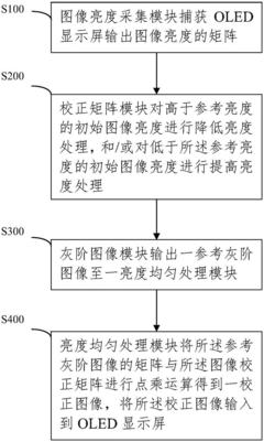
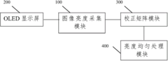
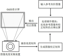
Method and device for improving display brightness uniformity of OLED (organic light emitting diode)
PatentActiveCN104599632A
Innovation
- The initial image brightness is captured through the image brightness acquisition module. The correction matrix module processes the initial image brightness that is higher or lower than the reference brightness, generates an image correction matrix, and performs a dot multiplication operation with the grayscale image module to generate a corrected image to improve the brightness. Uniformity.
Organic light emitting diode employing luminescent efficiency improvement layer
PatentActiveTW201016826A
Innovation
- Incorporation of a luminous efficiency improving layer containing a compound represented by Formula 1, which enhances the refractive index and facilitates constructive interference to improve light emission.
Quality Control Standards for OLED Manufacturing
Quality control standards in OLED manufacturing have evolved significantly to address the critical challenge of electroluminescent layer uniformity. These standards now incorporate multi-dimensional evaluation metrics that quantify both visual and functional uniformity aspects. The industry has established threshold values for luminance variation, typically allowing no more than ±5% deviation across the display area for premium products, with slightly relaxed standards of ±7-10% for consumer-grade applications.
Color uniformity standards have become increasingly stringent, with ΔE values (color difference metrics) below 2.0 considered imperceptible to the human eye and thus the gold standard for high-end displays. For mainstream consumer products, acceptable ΔE thresholds typically range between 2.0-3.5. These standards are complemented by specific chromaticity coordinate tolerances (Δx, Δy < 0.01) for professional applications.
Measurement protocols have been standardized across the industry, requiring specific environmental conditions: controlled temperature (23±1°C), humidity (40-60%), and dark room settings with minimal ambient light interference. The sampling methodology has also been formalized, with requirements for multiple measurement points (typically 9-25 points in a grid pattern) across the display surface to ensure comprehensive evaluation of uniformity.
Statistical process control (SPC) methods have been integrated into quality standards, establishing control limits for key uniformity parameters. These include Cpk (process capability index) values exceeding 1.33 for critical uniformity metrics, indicating a robust manufacturing process with minimal defect rates. Real-time monitoring systems now track these metrics throughout production, with automated alerts when parameters approach control limits.
International standardization bodies, including the International Electrotechnical Commission (IEC) and the Society for Information Display (SID), have developed specific test methods for OLED uniformity evaluation. These include IEC 62341-6-3 for luminance uniformity and chromaticity measurements. Major display manufacturers have also established their own proprietary standards that often exceed these international requirements, particularly for premium product lines.
Defect classification systems have been standardized to categorize uniformity issues by severity and visibility. These typically include mura defects (cloudy or uneven luminance), pixel defects, and color shifts, with specific acceptance criteria for each category based on defect size, location, and visibility under various viewing conditions.
Environmental Factors Affecting OLED Uniformity Measurements
Environmental conditions play a critical role in the accurate evaluation of OLED electroluminescent layer uniformity, potentially introducing significant measurement variations if not properly controlled. Temperature fluctuations represent one of the most impactful factors, as OLED materials exhibit temperature-dependent emission characteristics. Even minor temperature variations across a measurement setup can lead to non-uniform brightness patterns that may be misinterpreted as inherent device defects rather than measurement artifacts.
Humidity levels similarly affect measurement accuracy, particularly in non-encapsulated or inadequately sealed OLED devices. High humidity environments accelerate degradation mechanisms at the electroluminescent layer interfaces, creating localized dark spots or emission inconsistencies that compromise uniformity assessment. Industry standards typically recommend maintaining relative humidity below 40% during critical uniformity evaluations.
Ambient light contamination presents another significant challenge for precise uniformity measurements. Stray light can be reflected from the OLED surface or absorbed by the measurement equipment, introducing noise into the optical data. Best practices include conducting measurements in darkroom conditions with light-absorbing materials surrounding the test apparatus to minimize reflections and scattered light.
Electrostatic discharge (ESD) events, even at levels below human perception, can create permanent damage to OLED pixels or temporarily alter their emission characteristics. Comprehensive ESD protection protocols, including ionizing air systems and proper grounding of all measurement equipment, are essential for maintaining measurement integrity.
Airborne particulates represent an often overlooked environmental factor affecting uniformity measurements. Dust particles settling on either the OLED surface or optical measurement components can create shadows, diffraction patterns, or localized brightness variations. HEPA-filtered environments with positive pressure are increasingly becoming standard for high-precision uniformity evaluation systems.
Mechanical vibrations transmitted through building structures or nearby equipment can affect both the OLED device positioning and the optical measurement system alignment. These vibrations may introduce motion blur or misalignment artifacts in captured uniformity data. Advanced measurement setups typically incorporate vibration isolation tables or active damping systems to mitigate these effects.
Barometric pressure variations, while subtle in their impact, can affect the operating characteristics of certain measurement equipment, particularly when using vacuum-based cooling systems or when evaluating OLEDs in controlled atmosphere chambers. Calibration procedures should account for these variations to ensure measurement consistency across different environmental conditions.
Unlock deeper insights with PatSnap Eureka Quick Research — get a full tech report to explore trends and direct your research. Try now!
Generate Your Research Report Instantly with AI Agent
Supercharge your innovation with PatSnap Eureka AI Agent Platform!