

How to Improve PNP Transistor Integration in Complex Systems?
JUL 28, 20259 MIN READ
Generate Your Research Report Instantly with AI Agent
PatSnap Eureka helps you evaluate technical feasibility & market potential.
PNP Transistor Evolution
The evolution of PNP transistors has been a crucial aspect of semiconductor technology development since their inception in the mid-20th century. Initially, PNP transistors were the dominant type due to the ease of manufacturing with germanium as the semiconductor material. However, as silicon became the preferred material for transistor fabrication, NPN transistors gained prominence due to their superior performance characteristics.
The transition from germanium to silicon marked a significant milestone in PNP transistor evolution. Silicon-based PNP transistors offered improved temperature stability and higher operating frequencies compared to their germanium counterparts. This shift enabled the integration of PNP transistors into more complex circuits and systems, paving the way for advancements in analog and mixed-signal applications.
Throughout the 1970s and 1980s, efforts focused on enhancing PNP transistor performance through improved manufacturing processes and device structures. The introduction of epitaxial growth techniques allowed for better control of doping profiles, resulting in PNP transistors with higher current gain and lower parasitic capacitances. These improvements were crucial for expanding the use of PNP transistors in high-frequency applications and precision analog circuits.
The 1990s saw the emergence of complementary bipolar processes, which allowed for the simultaneous fabrication of high-performance NPN and PNP transistors on the same chip. This development was particularly important for the design of analog and mixed-signal circuits, as it enabled the creation of more symmetrical and balanced circuit topologies. The ability to integrate high-quality PNP transistors alongside NPN devices significantly expanded the design possibilities for complex systems.
In recent years, the evolution of PNP transistors has been driven by the need for higher integration density and improved power efficiency. Advanced manufacturing techniques, such as silicon-on-insulator (SOI) technology and vertical PNP structures, have been developed to address these challenges. These innovations have resulted in PNP transistors with reduced parasitic capacitances, improved frequency response, and better isolation from the substrate, making them more suitable for integration in modern complex systems.
The ongoing miniaturization of semiconductor devices has also impacted PNP transistor evolution. As feature sizes continue to shrink, new challenges emerge in maintaining device performance and reliability. Researchers and engineers are exploring novel materials and device architectures to overcome these limitations and push the boundaries of PNP transistor capabilities in nanoscale dimensions.
Looking ahead, the evolution of PNP transistors is likely to focus on further improving their integration in complex systems. This may involve developing new fabrication techniques to enhance compatibility with advanced CMOS processes, exploring three-dimensional integration strategies, and optimizing device characteristics for specific application domains such as high-speed communications, precision instrumentation, and power management circuits.
Market Demand Analysis
The market demand for improved PNP transistor integration in complex systems has been steadily growing, driven by the increasing complexity and miniaturization of electronic devices. As systems become more sophisticated, there is a pressing need for better performance, higher efficiency, and reduced power consumption in transistor-based circuits.
The automotive industry has emerged as a significant driver of this demand, with the rise of electric vehicles and advanced driver assistance systems requiring more complex and efficient electronic control units. Market research indicates that the automotive semiconductor market is expected to grow at a compound annual growth rate of over 8% in the next five years, with a substantial portion attributed to transistor technologies.
In the telecommunications sector, the rollout of 5G networks has created a surge in demand for high-performance transistors capable of operating at higher frequencies while maintaining low power consumption. This has led to increased interest in advanced PNP transistor designs that can be seamlessly integrated into complex radio frequency (RF) circuits.
The consumer electronics market continues to be a major contributor to the demand for improved PNP transistor integration. With the proliferation of Internet of Things (IoT) devices, smartphones, and wearables, there is a constant push for smaller form factors and longer battery life. This has resulted in a growing market for transistors that can deliver high performance in compact packages.
Industrial automation and control systems represent another significant market segment driving the need for better PNP transistor integration. As factories become smarter and more interconnected, there is an increasing demand for robust and efficient transistor solutions that can withstand harsh environments while providing precise control and monitoring capabilities.
The medical device industry has also shown a rising interest in advanced transistor technologies. With the trend towards miniaturization and portability in medical equipment, there is a growing need for highly integrated transistor solutions that can support complex diagnostic and therapeutic functions while maintaining low power consumption and high reliability.
Market analysts project that the global discrete semiconductor market, which includes transistors, will reach a value of over $30 billion by 2025. A significant portion of this growth is attributed to the demand for improved transistor technologies, including PNP transistors in complex systems.
The increasing focus on energy efficiency and sustainability across various industries has further fueled the demand for transistors with lower power dissipation and higher efficiency. This trend is particularly evident in the development of green technologies and renewable energy systems, where optimized transistor performance can significantly impact overall system efficiency.
Integration Challenges
The integration of PNP transistors into complex systems presents several significant challenges that must be addressed to improve overall system performance and reliability. One of the primary obstacles is the inherent slower switching speed of PNP transistors compared to their NPN counterparts. This speed limitation can create bottlenecks in high-frequency applications, potentially compromising the system's overall efficiency and responsiveness.
Another critical challenge lies in the thermal management of PNP transistors within densely packed circuits. As complex systems often require a high degree of integration, the heat generated by PNP transistors can lead to localized hot spots, potentially affecting the performance and lifespan of surrounding components. This necessitates careful consideration of thermal design and layout strategies to ensure optimal heat dissipation.
The issue of parasitic capacitance also poses a significant hurdle in PNP transistor integration. In complex systems, the proximity of components can lead to increased parasitic capacitance, which may result in signal degradation and unwanted coupling between circuit elements. Mitigating these effects requires sophisticated layout techniques and potentially the use of advanced isolation technologies.
Furthermore, the voltage requirements of PNP transistors can complicate power management in complex systems. PNP transistors typically require a negative voltage supply, which may necessitate additional power rails or voltage conversion circuitry, adding to the overall complexity and power consumption of the system.
Noise susceptibility is another challenge that engineers must contend with when integrating PNP transistors. In mixed-signal environments, PNP transistors can be more susceptible to noise interference, potentially compromising signal integrity and system performance. This requires careful consideration of shielding techniques and circuit isolation strategies.
The manufacturing process for PNP transistors also presents integration challenges. Achieving consistent performance across a large number of PNP transistors in a complex system can be difficult due to variations in the manufacturing process. This variability can lead to mismatches in transistor characteristics, potentially affecting the overall system behavior and reliability.
Lastly, the size and layout constraints of complex systems can make it challenging to incorporate PNP transistors effectively. As miniaturization continues to drive the development of electronic systems, finding ways to integrate PNP transistors without compromising on performance or increasing the overall footprint becomes increasingly difficult. This challenge requires innovative approaches to circuit design and layout optimization to maximize the utilization of available space while maintaining the desired electrical characteristics.
Current Integration Methods
01 Fabrication techniques for PNP transistors
Various methods for manufacturing PNP transistors in integrated circuits, including epitaxial growth, ion implantation, and diffusion processes. These techniques aim to optimize the transistor's performance and integration density within semiconductor devices.- Fabrication techniques for PNP transistors: Various methods for manufacturing PNP transistors in integrated circuits, including epitaxial growth, ion implantation, and diffusion processes. These techniques aim to optimize the transistor's performance and integration density within semiconductor devices.
- PNP transistor structure optimization: Design improvements in PNP transistor structures to enhance their electrical characteristics, such as current gain, breakdown voltage, and frequency response. This includes modifications to the emitter, base, and collector regions, as well as the introduction of specialized layers or geometries.
- Integration of PNP transistors with other components: Techniques for integrating PNP transistors with other semiconductor components, such as NPN transistors, resistors, and capacitors, to create complex integrated circuits. This includes methods for isolating different components and optimizing their layout for improved performance and reduced chip area.
- PNP transistor applications in analog circuits: Utilization of PNP transistors in various analog circuit designs, such as current mirrors, voltage references, and amplifiers. These applications leverage the unique characteristics of PNP transistors to achieve specific circuit functionalities and performance goals.
- PNP transistor modeling and simulation: Development of accurate models and simulation techniques for PNP transistors to predict their behavior in integrated circuits. This includes the creation of compact models, parameter extraction methods, and simulation tools to aid in the design and optimization of PNP-based circuits.
02 PNP transistor structures in integrated circuits
Design and implementation of PNP transistor structures in integrated circuits, focusing on vertical and lateral configurations. These structures are optimized for specific applications and to improve overall circuit performance.Expand Specific Solutions03 Integration of PNP transistors with other components
Techniques for integrating PNP transistors with other semiconductor components such as NPN transistors, resistors, and capacitors. This integration aims to create more complex and functional integrated circuits while minimizing chip area and power consumption.Expand Specific Solutions04 PNP transistor applications in analog and digital circuits
Implementation of PNP transistors in various analog and digital circuit applications, including amplifiers, current mirrors, and logic gates. These applications leverage the unique characteristics of PNP transistors to enhance circuit performance and functionality.Expand Specific Solutions05 Optimization of PNP transistor characteristics
Methods for improving PNP transistor characteristics such as current gain, frequency response, and noise performance. These optimizations involve adjusting doping profiles, geometry, and other parameters to enhance the overall performance of integrated circuits containing PNP transistors.Expand Specific Solutions
Key Industry Players
The integration of PNP transistors in complex systems is a mature technology, but continuous improvement efforts are ongoing in a highly competitive market. The industry is in a phase of optimization and refinement, with major players like Infineon Technologies, GlobalFoundries, and STMicroelectronics leading the way. The market size is substantial, driven by the increasing demand for high-performance analog and mixed-signal circuits in various applications. Technologically, companies are focusing on enhancing PNP transistor performance, reducing parasitic effects, and improving integration density. IBM and Texas Instruments are also contributing significantly to advancements in this field, leveraging their extensive semiconductor expertise and research capabilities.
Infineon Technologies AG
Technical Solution: Infineon has developed advanced PNP transistor integration techniques for complex systems, focusing on their CoolSiC™ MOSFET technology. They have implemented a unique trench design that allows for higher cell density and lower on-resistance[1]. This design incorporates PNP structures to enhance overall performance. Infineon's approach includes the use of advanced epitaxial growth techniques to create precise doping profiles, which is crucial for PNP transistor functionality in high-voltage applications[2]. They have also introduced innovative packaging solutions, such as TO-Leadless (TOLL) packages, which improve thermal management and allow for better integration of PNP transistors in compact designs[3].
Strengths: Superior thermal management, high voltage handling capability, and compact design integration. Weaknesses: Potentially higher production costs due to advanced manufacturing processes and specialized packaging requirements.
International Business Machines Corp.
Technical Solution: IBM has made significant strides in PNP transistor integration through their Silicon Germanium (SiGe) BiCMOS technology. This approach allows for the creation of high-performance PNP transistors alongside traditional CMOS structures on a single chip[4]. IBM's technique involves the precise deposition of SiGe layers to create a heterojunction bipolar transistor (HBT) structure, which enhances the performance of PNP transistors in terms of speed and power efficiency[5]. They have also developed advanced wafer-level packaging techniques that enable 3D integration of PNP transistors, significantly improving overall system density and performance[6]. IBM's research has shown that their SiGe PNP transistors can achieve cutoff frequencies exceeding 300 GHz, making them suitable for high-frequency applications in complex systems[7].
Strengths: High-frequency performance, compatibility with CMOS processes, and potential for 3D integration. Weaknesses: Higher manufacturing complexity and potentially increased production costs compared to standard silicon processes.
Core PNP Innovations
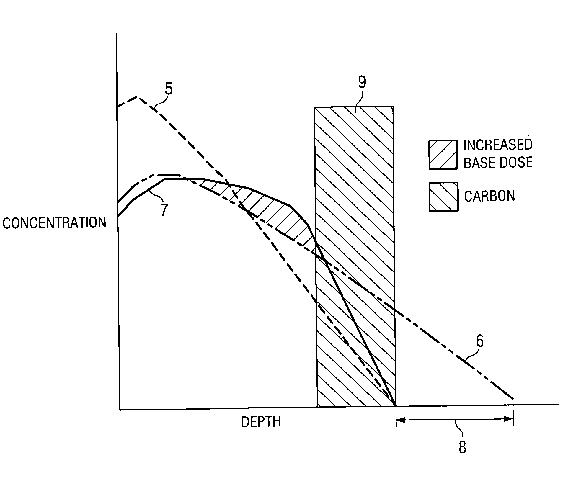
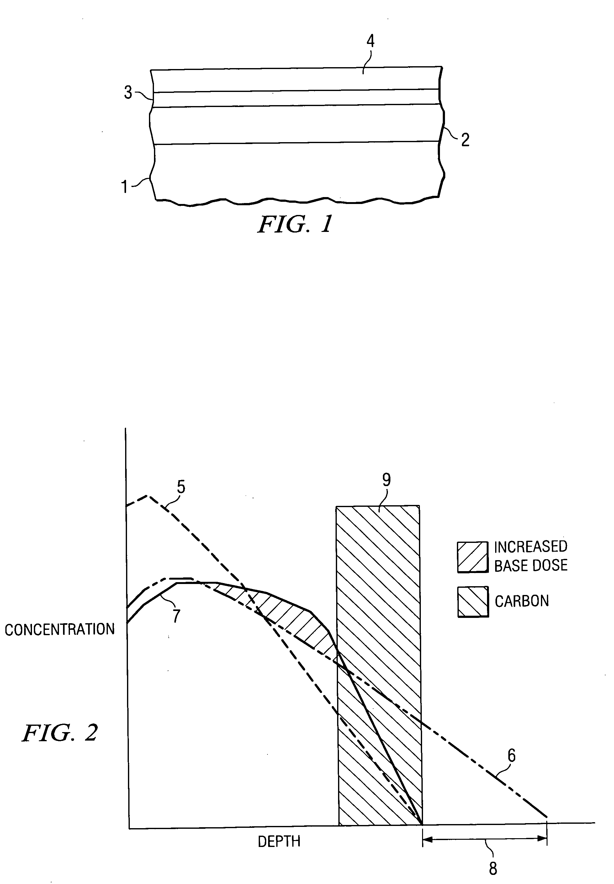
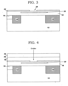
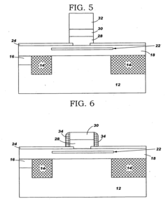
Control of phosphorus profile by carbon in-situ doping for high performance vertical PNP transistor
PatentInactiveUS20050118771A1
Innovation
- Incorporating carbon into the base layer only in the vicinity of the collector-base junction zone to suppress phosphorous diffusion, allowing for a high surface concentration of phosphorous that diffuses towards the junction zone while preventing further diffusion into the collector layer, thereby maintaining a narrow base profile.
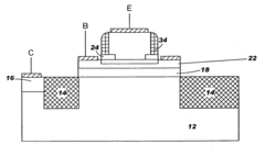
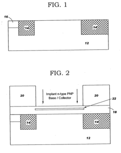
High performance integrated vertical transistors and method of making the same
PatentInactiveUS20070001264A1
Innovation
- The use of a shared silicon germanium (SiGe) low temperature epitaxial (LTE) layer allows for the fabrication of vertically aligned complementary bipolar transistors, where the NPN and PNP transistors share the same epitaxial base and collector regions, with the PNP emitter layer acting as the NPN base layer, utilizing advanced epitaxial techniques like molecular beam epitaxy (MBE) and low temperature epitaxy (LTE) to ensure identical vertical profiles.
Thermal Management
Thermal management is a critical aspect of improving PNP transistor integration in complex systems. As transistor density increases and power requirements grow, effective heat dissipation becomes paramount to ensure optimal performance and reliability. The thermal challenges associated with PNP transistors stem from their inherent power dissipation characteristics and the compact nature of modern integrated circuits.
One of the primary approaches to thermal management in PNP transistor integration is the implementation of advanced packaging techniques. These include the use of thermally conductive materials, such as copper-based substrates or diamond-filled composites, to enhance heat transfer from the transistor junctions to the package exterior. Additionally, the incorporation of heat spreaders and heat sinks within the package design can significantly improve thermal dissipation capabilities.
On-chip thermal management strategies play a crucial role in mitigating localized hot spots and maintaining uniform temperature distribution across the integrated circuit. Techniques such as dynamic thermal management (DTM) and adaptive voltage scaling (AVS) can be employed to adjust transistor operation based on real-time temperature measurements. These methods help prevent thermal runaway and extend the operational lifespan of PNP transistors in complex systems.
The integration of microfluidic cooling channels within the semiconductor substrate represents an innovative approach to thermal management. By circulating coolant through microscale channels etched into the silicon, heat can be efficiently removed from critical areas of the integrated circuit. This technique offers the potential for significant improvements in thermal performance, particularly in high-power applications where traditional air cooling methods may be insufficient.
Advanced thermal simulation and modeling tools are essential for optimizing the thermal design of complex systems incorporating PNP transistors. Computational fluid dynamics (CFD) simulations and finite element analysis (FEA) enable engineers to predict thermal behavior and identify potential hot spots before physical prototyping. These tools facilitate the development of more effective thermal management strategies and help reduce design iterations.
Emerging technologies such as phase-change materials (PCMs) and thermoelectric coolers (TECs) offer promising solutions for enhancing thermal management in PNP transistor integration. PCMs can absorb and store excess heat during peak operation, while TECs provide localized cooling capabilities through the Peltier effect. The integration of these technologies into complex systems can significantly improve thermal performance and enable higher levels of transistor integration.
Reliability Assessment
Reliability assessment is a critical aspect of improving PNP transistor integration in complex systems. The performance and longevity of these systems heavily depend on the reliability of their components, particularly transistors. PNP transistors, being fundamental building blocks in many electronic circuits, require thorough evaluation to ensure their consistent operation under various conditions.
One key factor in assessing PNP transistor reliability is thermal stability. Complex systems often operate in environments with fluctuating temperatures, which can significantly impact transistor performance. Rigorous thermal cycling tests are essential to evaluate how PNP transistors respond to temperature variations, ensuring they maintain their electrical characteristics across a wide range of operating conditions.
Another crucial aspect is electrical stress testing. PNP transistors in complex systems may be subjected to voltage and current spikes, which can lead to degradation or failure over time. Accelerated life testing techniques, such as high-temperature operating life (HTOL) tests, can provide valuable insights into the long-term reliability of these components under extreme electrical conditions.
Moisture sensitivity is also a significant concern in PNP transistor reliability. Complex systems may be exposed to varying humidity levels, potentially leading to corrosion or other moisture-related issues. Implementing proper moisture barrier techniques and conducting humidity tests are essential steps in ensuring the longevity of PNP transistors in these systems.
Electrostatic discharge (ESD) protection is another critical factor in reliability assessment. PNP transistors can be particularly sensitive to ESD events, which can cause immediate failure or latent damage. Implementing robust ESD protection measures and conducting thorough ESD testing are vital for improving the overall reliability of complex systems incorporating these transistors.
Radiation hardness is an important consideration for systems operating in environments with high levels of electromagnetic interference or ionizing radiation. Assessing the radiation tolerance of PNP transistors and implementing appropriate shielding techniques can significantly enhance the reliability of complex systems in such challenging environments.
Lastly, reliability assessment should include a comprehensive analysis of failure modes and effects. This involves identifying potential failure mechanisms specific to PNP transistors in complex systems and developing strategies to mitigate these risks. Techniques such as Failure Mode and Effects Analysis (FMEA) can be invaluable in this process, helping to prioritize reliability improvement efforts and optimize system design for enhanced longevity and performance.
Unlock deeper insights with PatSnap Eureka Quick Research — get a full tech report to explore trends and direct your research. Try now!
Generate Your Research Report Instantly with AI Agent
Supercharge your innovation with PatSnap Eureka AI Agent Platform!