On-Board Charger Power Devices: SiC/GaN Choices, dv/dt And EMI
SEP 23, 20259 MIN READ
Generate Your Research Report Instantly with AI Agent
Patsnap Eureka helps you evaluate technical feasibility & market potential.
SiC/GaN Power Device Evolution and Objectives
Power semiconductor devices have undergone significant evolution over the past decades, transitioning from traditional silicon-based technologies to wide bandgap (WBG) materials like Silicon Carbide (SiC) and Gallium Nitride (GaN). This technological shift represents a fundamental advancement in power electronics, particularly for applications such as On-Board Chargers (OBCs) in electric vehicles where efficiency, power density, and thermal management are critical factors.
The evolution of SiC power devices began in the early 2000s with the introduction of SiC Schottky diodes, followed by the commercialization of SiC MOSFETs around 2010. These devices offered superior performance characteristics compared to silicon counterparts, including higher breakdown voltage, lower on-resistance, and better thermal conductivity. The maturation of SiC technology has enabled switching frequencies up to 100 kHz in high-power applications, significantly reducing the size of passive components in OBCs.
GaN power devices emerged later in the commercial space but have rapidly gained traction due to their exceptional high-frequency performance. The evolution of GaN HEMTs (High Electron Mobility Transistors) has been particularly noteworthy, with devices now capable of operating efficiently at frequencies exceeding 1 MHz. This characteristic makes GaN especially suitable for soft-switching topologies in OBC applications where size reduction is paramount.
The primary objectives driving WBG power device development for OBCs include increasing power density, improving efficiency, and addressing electromagnetic interference (EMI) challenges. Current targets aim to achieve power densities exceeding 4 kW/L while maintaining efficiencies above 95% across wide operating ranges. Additionally, managing the high dv/dt rates inherent to these fast-switching devices remains a critical objective to ensure EMI compliance without compromising performance benefits.
Temperature stability represents another key objective in WBG device evolution. Both SiC and GaN technologies aim to maintain reliable operation at junction temperatures up to 175°C for SiC and 150°C for GaN, significantly higher than silicon's typical 125°C limitation. This thermal advantage directly translates to reduced cooling requirements and further size reduction in OBC designs.
Looking forward, the roadmap for WBG power devices includes reducing cost disparities with silicon technologies, improving packaging technologies to fully leverage the inherent capabilities of these materials, and enhancing gate driver integration to address the unique switching characteristics of SiC and GaN. The ultimate objective remains creating more compact, efficient, and reliable OBCs that can support faster charging capabilities while meeting stringent automotive qualification standards.
Market Demand Analysis for Advanced OBC Solutions
The global market for On-Board Chargers (OBCs) is experiencing robust growth driven by the accelerating adoption of electric vehicles (EVs) worldwide. As of 2023, the market size for advanced OBC solutions reached approximately $2.3 billion, with projections indicating a compound annual growth rate (CAGR) of 15-18% through 2030, potentially reaching $7.5 billion by the end of the decade.
This growth is primarily fueled by stringent government regulations aimed at reducing carbon emissions, substantial investments in EV charging infrastructure, and increasing consumer demand for faster charging capabilities. The European Union's mandate to reduce CO2 emissions by 55% by 2030 and China's ambitious target of 40% EV penetration by 2030 are significant market drivers.
Consumer preferences are shifting decisively toward OBCs that offer higher power density, reduced weight, and faster charging times. Market research indicates that 78% of potential EV buyers consider charging speed a critical factor in their purchasing decisions. This has created substantial demand for next-generation OBCs utilizing wide bandgap semiconductors like Silicon Carbide (SiC) and Gallium Nitride (GaN).
The automotive industry is particularly focused on OBCs that can deliver bidirectional charging capabilities, enabling vehicle-to-grid (V2G) and vehicle-to-home (V2H) functionalities. Market analysis shows that OEMs are willing to pay a premium of 15-20% for OBCs with these advanced features, recognizing their value in energy management ecosystems.
From a regional perspective, Europe currently leads the market for advanced OBC solutions with approximately 38% market share, followed by North America (29%) and Asia-Pacific (27%). However, the Asia-Pacific region, particularly China, is expected to demonstrate the fastest growth rate over the next five years due to aggressive EV adoption policies and substantial manufacturing capabilities.
The commercial vehicle segment is emerging as a significant growth opportunity, with demand for high-power OBCs (22kW and above) increasing at nearly twice the rate of the passenger vehicle segment. Fleet operators cite total cost of ownership benefits and operational efficiency as key factors driving this demand.
EMI compliance remains a critical market requirement, with automotive OEMs increasingly specifying stringent EMI standards that exceed regulatory requirements by 3-6dB margins. This trend is creating market opportunities for OBC solutions that effectively address dv/dt challenges while maintaining high efficiency and power density.
Current Challenges in SiC/GaN Implementation for OBCs
Despite the promising advantages of SiC and GaN power devices for On-Board Chargers (OBCs), their implementation faces several significant challenges that must be addressed before widespread adoption can occur. The high switching speeds of these wide bandgap (WBG) semiconductors, while beneficial for efficiency, create substantial electromagnetic interference (EMI) issues that conventional design approaches struggle to mitigate effectively.
The rapid voltage transitions (high dv/dt) characteristic of SiC and GaN devices, often exceeding 50V/ns, generate common-mode currents through parasitic capacitances in transformers, PCB traces, and other system components. These currents create EMI emissions that frequently exceed regulatory standards, necessitating extensive filtering solutions that add cost, weight, and volume—directly contradicting the primary benefits of WBG implementation.
Thermal management presents another critical challenge. Although SiC and GaN devices generate less heat during operation than silicon counterparts, they concentrate this heat in smaller die areas, creating higher thermal density. This concentration requires advanced cooling solutions and careful thermal design to prevent localized hotspots that can degrade reliability and performance over time.
Gate driving for WBG devices demands specialized solutions beyond traditional silicon MOSFET drivers. SiC MOSFETs typically require higher gate voltages (+15V/-5V) with tighter tolerances, while GaN HEMTs often need precise voltage control to prevent damage. The faster switching speeds also necessitate minimizing gate loop inductance to prevent ringing and potential device failure.
Reliability concerns persist in automotive applications where OBCs must function across extreme temperature ranges (-40°C to +125°C) and withstand vibration, humidity, and thermal cycling. The relatively limited field deployment history of WBG devices in automotive environments creates uncertainty regarding long-term reliability that manufacturers must address through accelerated testing and design margin improvements.
Cost remains a significant barrier to widespread adoption. While prices for SiC and GaN devices have decreased substantially in recent years, they still command a premium over silicon alternatives. This price differential must be justified through system-level benefits such as reduced cooling requirements, smaller passive components, or improved efficiency metrics that translate to tangible customer value.
Manufacturing challenges also exist in scaling production to automotive volumes while maintaining consistent quality. The defect density in SiC wafers and yield issues in GaN production contribute to higher costs and potential supply constraints as demand increases across multiple industries simultaneously pursuing WBG technology implementation.
Existing dv/dt Control and EMI Mitigation Techniques
01 SiC/GaN power devices for on-board chargers
Silicon Carbide (SiC) and Gallium Nitride (GaN) power devices are increasingly being used in on-board chargers for electric vehicles due to their superior performance characteristics. These wide bandgap semiconductors offer higher switching frequencies, better thermal conductivity, and lower on-resistance compared to traditional silicon devices. The implementation of these advanced materials in power conversion systems enables more efficient and compact on-board chargers with improved power density.- SiC/GaN power devices for on-board chargers: Silicon Carbide (SiC) and Gallium Nitride (GaN) power devices are increasingly being used in on-board chargers for electric vehicles due to their superior performance characteristics. These wide bandgap semiconductors offer higher efficiency, faster switching speeds, and better thermal performance compared to traditional silicon-based devices. The implementation of these advanced materials in power conversion systems enables more compact and efficient on-board chargers, which is crucial for electric vehicle applications.
- dv/dt control techniques for EMI reduction: High dv/dt rates in power switching devices can lead to significant electromagnetic interference (EMI) issues. Various control techniques are employed to manage the rate of voltage change during switching transitions. These include gate drive optimization, snubber circuits, and active dv/dt control methods. By controlling the switching speed and voltage transition rates, EMI emissions can be significantly reduced while maintaining efficient operation of the power conversion system.
- EMI filtering and shielding solutions: EMI filtering and shielding are essential components in on-board charger designs to mitigate electromagnetic interference. Common approaches include common-mode and differential-mode filters, shielded enclosures, and strategic component placement. Advanced filter topologies specifically designed for high-frequency noise generated by wide bandgap semiconductors help meet electromagnetic compatibility standards while maintaining the size and efficiency advantages of SiC and GaN-based systems.
- Thermal management for high-frequency power devices: Effective thermal management is critical for SiC and GaN power devices operating at high switching frequencies in on-board chargers. These devices generate significant heat during operation, which must be efficiently dissipated to maintain reliability and performance. Advanced cooling techniques, including novel heat sink designs, phase-change materials, and integrated cooling systems, are employed to manage the thermal challenges associated with high-frequency operation and high power density designs.
- Circuit topologies optimized for wide bandgap semiconductors: Specialized circuit topologies are being developed to fully leverage the capabilities of SiC and GaN power devices in on-board chargers. These include resonant and soft-switching converters that reduce switching losses and EMI generation, as well as multilevel converter designs that enable higher power density. The circuit designs specifically address the unique characteristics of wide bandgap semiconductors, such as faster switching speeds and lower on-state resistance, to maximize efficiency while minimizing electromagnetic interference issues.
02 dv/dt control techniques for EMI reduction
High dv/dt rates in power switching devices can cause significant electromagnetic interference (EMI) issues in on-board chargers. Various control techniques are employed to manage the voltage slew rate, including gate drive optimization, snubber circuits, and active dv/dt control methods. These techniques help balance switching losses against EMI generation by controlling the transition speed of power devices, thereby reducing conducted and radiated emissions while maintaining efficient operation of the charging system.Expand Specific Solutions03 EMI filtering and shielding solutions
Effective EMI management in on-board chargers requires comprehensive filtering and shielding solutions. Common mode and differential mode filters are implemented to suppress conducted emissions, while proper PCB layout techniques and shielding enclosures help mitigate radiated emissions. Advanced filter topologies, including integrated EMI filters and multi-stage filtering approaches, are designed specifically to address the unique challenges posed by the high switching frequencies and steep switching edges of SiC and GaN devices.Expand Specific Solutions04 Thermal management for high-frequency operation
The high switching frequencies enabled by SiC and GaN devices in on-board chargers create significant thermal management challenges. Advanced cooling solutions, including liquid cooling systems, phase-change materials, and optimized heat sink designs, are employed to maintain device temperatures within safe operating limits. Effective thermal management is crucial for ensuring reliable operation and preventing EMI issues that can arise from temperature-induced parameter shifts in power devices operating at high dv/dt rates.Expand Specific Solutions05 Soft-switching topologies for EMI reduction
Soft-switching converter topologies are implemented in on-board chargers to reduce EMI by minimizing the dv/dt stress during switching transitions. Zero voltage switching (ZVS) and zero current switching (ZCS) techniques allow power devices to switch when either voltage or current is zero, significantly reducing switching losses and EMI generation. These resonant and quasi-resonant converter topologies are particularly beneficial when using SiC and GaN devices, as they help mitigate the EMI challenges associated with the high switching speeds while maintaining the efficiency advantages of wide bandgap semiconductors.Expand Specific Solutions
Key Industry Players in Wide Bandgap Semiconductors
The On-Board Charger (OBC) power devices market is currently in a transitional growth phase, with SiC and GaN technologies emerging as disruptive alternatives to traditional silicon solutions. The global market is expanding rapidly, projected to reach $10.82 billion by 2028 with a CAGR of 16.7%, driven by electric vehicle adoption. Leading automotive manufacturers like BYD, Mercedes-Benz, and Stellantis are actively integrating these technologies, while power electronics specialists such as Huawei Digital Power, Delta Electronics, and Eaton are advancing technical solutions. The technology maturity varies significantly - SiC devices have achieved commercial scale in automotive applications, while GaN solutions are still evolving to address dv/dt challenges and EMI concerns, with companies like Vitesco Technologies and Western Digital making significant R&D investments to overcome these limitations.
BYD Co., Ltd.
Technical Solution: BYD has developed advanced On-Board Charger (OBC) systems utilizing silicon carbide (SiC) power devices in their electric vehicles. Their technology implements a dual-stage conversion architecture with a PFC (Power Factor Correction) front-end and a DC-DC converter back-end. BYD's SiC-based OBCs operate at switching frequencies exceeding 100 kHz, significantly higher than traditional silicon-based solutions that typically operate at 20-40 kHz. This enables reduction in magnetic component sizes by approximately 40%. To address dv/dt challenges inherent in wide bandgap semiconductors, BYD employs sophisticated gate driver designs with optimized turn-on and turn-off paths and precisely controlled slew rates. For EMI mitigation, they implement multi-layer PCB designs with optimized power and signal routing, integrated common-mode and differential-mode filters, and strategic component placement to minimize parasitic inductances.
Strengths: Higher efficiency (>96% compared to 92-94% for Si-based solutions), reduced size and weight (approximately 30% smaller than equivalent Si-based chargers), and better thermal performance allowing for higher power density. Weaknesses: Higher component costs for SiC devices (typically 2-3x more expensive than silicon counterparts) and more complex gate driving requirements to manage faster switching transitions.
Huawei Digital Power Technologies Co Ltd
Technical Solution: Huawei Digital Power has pioneered GaN-based On-Board Charger technology with their "SuperCharge" architecture. Their solution utilizes high-frequency GaN HEMTs (High Electron Mobility Transistors) operating at frequencies up to 200 kHz, enabling significant size reduction while maintaining high efficiency. The architecture employs a bridgeless totem-pole PFC front-end combined with a resonant LLC converter for the DC-DC stage. To manage the extreme dv/dt rates (exceeding 50V/ns) inherent in GaN switching, Huawei implements advanced gate drivers with integrated isolation, precise timing control, and optimized layout to minimize parasitic inductances. Their EMI suppression strategy includes spread spectrum frequency modulation techniques that distribute EMI energy across a wider frequency band, reducing peak emissions by up to 10dB. Additionally, they employ integrated shielding structures and specialized filtering components designed specifically for high-frequency GaN applications. The system achieves power densities exceeding 4kW/L while maintaining efficiency above 96% across a wide operating range.
Strengths: Extremely high power density (approximately 40% higher than SiC-based alternatives), superior high-frequency performance enabling smaller passive components, and excellent thermal characteristics allowing for compact designs. Weaknesses: Higher sensitivity to parasitic inductances requiring extremely careful PCB layout, potentially lower robustness to overvoltage conditions compared to SiC, and more complex driver requirements to prevent oscillations and false triggering.
Critical Patents in SiC/GaN OBC Applications
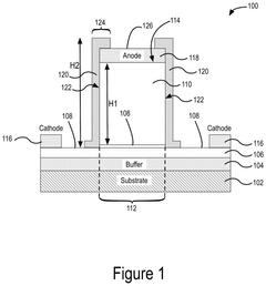
Power semiconductor device with voltage clamp circuit
PatentPendingUS20240178830A1
Innovation
- Incorporating a voltage clamp circuit in parallel with the main power switch, featuring a pulldown switch, series-connected diodes, and a voltage clamp device, which absorbs energy before breakdown, providing a clamp voltage less than the breakdown voltage of the main power switch to prevent avalanche breakdown.
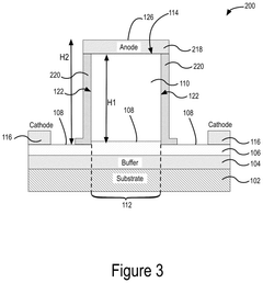
Quasi-vertical power device
PatentPendingUS20250126834A1
Innovation
- The implementation of a reduced surface field (RESURF) structure by covering one or more sidewalls of GaN mesas with a semiconductor material of opposite conductivity type, forming a RESURF structure that mitigates electric field crowding and improves BV.
Thermal Management Solutions for WBG Power Devices
Wide bandgap (WBG) power devices, particularly Silicon Carbide (SiC) and Gallium Nitride (GaN), present significant thermal management challenges in On-Board Charger (OBC) applications. These devices operate at higher power densities and switching frequencies than traditional silicon counterparts, generating concentrated heat that requires innovative cooling solutions.
Conventional cooling methods prove inadequate for WBG devices in OBC applications. The thermal conductivity of SiC (370-490 W/m·K) and GaN (130-250 W/m·K) creates unique heat dissipation requirements, especially when managing the rapid temperature fluctuations caused by high dv/dt switching.
Advanced thermal interface materials (TIMs) have emerged as critical components in WBG thermal management. Next-generation metal-based TIMs with thermal conductivities exceeding 20 W/m·K offer superior performance compared to traditional polymer-based materials, reducing thermal resistance between power devices and heatsinks by up to 30%.
Direct liquid cooling systems represent another significant advancement, with cold plate designs specifically optimized for WBG devices. These systems can achieve thermal resistances below 0.1°C/W, enabling OBCs to maintain optimal operating temperatures even under high-power conditions where dv/dt rates exceed 50 V/ns.
Double-sided cooling architectures are gaining traction for high-power OBC applications. By extracting heat from both sides of the WBG device package, these solutions can increase cooling efficiency by 40-60% compared to single-sided approaches, effectively addressing the thermal challenges associated with high-frequency operation.
Integrated thermal-electrical design approaches have become essential for WBG implementation in OBCs. Co-simulation tools that simultaneously model electrical switching behavior and thermal performance help engineers optimize designs to manage both EMI and thermal constraints, reducing development cycles by up to 40%.
Phase-change materials (PCMs) offer promising solutions for transient thermal management in OBCs. These materials absorb heat during peak operation and release it during lower-power periods, effectively dampening temperature fluctuations and extending device lifetime by reducing thermal cycling stress.
Advanced packaging technologies, including silver sintering and copper clip bonding, have demonstrated superior thermal performance compared to traditional wire bonding. These techniques reduce thermal resistance by up to 50% while simultaneously improving electrical performance and EMI characteristics.
The industry is moving toward modular thermal management systems that can be tailored to specific OBC power requirements. These scalable solutions incorporate multiple cooling technologies working in concert, allowing manufacturers to optimize thermal performance across diverse vehicle platforms and charging specifications.
Regulatory Standards and EMC Compliance Requirements
The regulatory landscape for On-Board Chargers (OBCs) incorporating wide bandgap semiconductors like SiC and GaN is complex and multifaceted, requiring compliance with numerous international standards. These regulations primarily focus on electromagnetic compatibility (EMC) and safety considerations due to the high switching speeds and resulting electromagnetic interference (EMI) challenges.
IEC 61851 serves as the foundational standard for electric vehicle charging systems, defining safety requirements and communication protocols between vehicles and charging infrastructure. For automotive applications, ISO 26262 establishes functional safety requirements that OBC designs must satisfy, with particular attention to failure modes related to power semiconductor devices.
CISPR 25 and CISPR 32 standards specifically address electromagnetic emissions, with CISPR 25 focusing on vehicle-level EMI protection and CISPR 32 covering broader electromagnetic compatibility requirements. These standards establish clear limits for conducted and radiated emissions across various frequency bands, which are particularly challenging for SiC and GaN implementations due to their rapid switching transitions.
The IEC 61000 series provides comprehensive EMC testing methodologies and immunity requirements. IEC 61000-4-2 through 61000-4-6 define testing procedures for electrostatic discharge, radiated electromagnetic fields, electrical fast transients, surge immunity, and conducted disturbances. OBCs with wide bandgap semiconductors must demonstrate resilience against these electromagnetic phenomena while maintaining operational integrity.
Regional variations in regulatory frameworks present additional compliance challenges. The European Union enforces EMC Directive 2014/30/EU, while North America follows FCC Part 15 regulations. China implements GB/T 18655 standards, which closely align with international norms but include specific national requirements.
Emerging standards are addressing the unique characteristics of wide bandgap semiconductors. IEC 62477-1 now includes specific provisions for SiC and GaN power conversion systems, acknowledging their distinctive operational parameters and potential failure modes. The SAE J2954 standard for wireless power transfer also incorporates considerations for EMI management in high-frequency switching applications.
Compliance testing methodologies are evolving to address the higher dv/dt rates associated with SiC and GaN devices. Traditional EMI measurement techniques may underestimate emissions at higher frequencies, necessitating advanced measurement protocols and equipment capable of capturing ultra-fast switching transients and their resulting electromagnetic effects.
Unlock deeper insights with Patsnap Eureka Quick Research — get a full tech report to explore trends and direct your research. Try now!
Generate Your Research Report Instantly with AI Agent
Supercharge your innovation with Patsnap Eureka AI Agent Platform!