Tautomerization in Interactional Nanostructures: Sensors and Devices
JUL 29, 20259 MIN READ
Generate Your Research Report Instantly with AI Agent
Patsnap Eureka helps you evaluate technical feasibility & market potential.
Tautomerization Fundamentals and Objectives
Tautomerization, a fundamental concept in organic chemistry, plays a crucial role in the development of interactional nanostructures for sensors and devices. This phenomenon involves the rapid interconversion between structural isomers, known as tautomers, which differ in the position of a proton and a π bond. The study of tautomerization in nanostructures has gained significant attention due to its potential applications in molecular switches, sensors, and electronic devices.
The evolution of tautomerization research can be traced back to the early 20th century, with pioneering work by chemists such as Linus Pauling and Johannes Thiele. However, it is only in recent decades that the importance of tautomerization in nanoscale systems has been fully recognized. The advent of advanced spectroscopic techniques and computational methods has enabled researchers to investigate tautomerization processes at unprecedented levels of detail.
In the context of interactional nanostructures, tautomerization offers unique opportunities for designing responsive and adaptive materials. The ability of certain molecules to switch between tautomeric forms in response to external stimuli, such as light, pH, or electric fields, provides a molecular-level mechanism for signal transduction and information processing. This property is particularly valuable in the development of sensors and devices that can detect and respond to environmental changes with high sensitivity and specificity.
The primary objectives of studying tautomerization in interactional nanostructures are multifaceted. First, researchers aim to gain a deeper understanding of the fundamental mechanisms governing tautomeric transitions at the nanoscale. This includes elucidating the energetics, kinetics, and quantum mechanical aspects of proton transfer processes in confined environments. Second, there is a strong focus on developing novel materials and architectures that can exploit tautomerization for practical applications.
Another key objective is to explore the integration of tautomeric systems into functional devices. This involves designing nanostructures that can harness tautomerization to perform specific tasks, such as molecular recognition, chemical sensing, or logic operations. Researchers are also investigating ways to control and manipulate tautomerization processes with external stimuli, paving the way for the development of switchable and reconfigurable nanodevices.
Furthermore, the field aims to bridge the gap between fundamental research and practical applications. This includes addressing challenges related to the stability, reproducibility, and scalability of tautomeric nanostructures. Efforts are underway to develop robust fabrication techniques and characterization methods that can translate laboratory discoveries into commercially viable technologies.
As the field progresses, interdisciplinary collaboration becomes increasingly important. The study of tautomerization in interactional nanostructures draws upon expertise from chemistry, physics, materials science, and engineering. This convergence of disciplines is driving innovation and opening up new avenues for technological advancement in areas such as biosensing, drug delivery, and nanoelectronics.
Market Analysis for Nanostructure-based Sensors
The market for nanostructure-based sensors is experiencing rapid growth, driven by increasing demand across various industries. These sensors, which leverage the unique properties of nanomaterials, offer enhanced sensitivity, selectivity, and miniaturization compared to traditional sensing technologies. The global market for nanosensors is projected to reach significant value in the coming years, with a compound annual growth rate (CAGR) outpacing many other technology sectors.
Key industries driving this market growth include healthcare, environmental monitoring, food safety, and industrial process control. In healthcare, nanostructure-based sensors are revolutionizing diagnostics, enabling rapid and accurate detection of biomarkers for various diseases. The environmental sector is adopting these sensors for real-time monitoring of air and water quality, addressing growing concerns about pollution and climate change.
The food industry is increasingly utilizing nanosensors for quality control and safety assurance, detecting contaminants and ensuring product integrity throughout the supply chain. In industrial applications, these sensors are enhancing process efficiency and safety by providing precise measurements in challenging environments.
Geographically, North America and Europe currently lead the market, benefiting from advanced research infrastructure and strong investment in nanotechnology. However, the Asia-Pacific region is expected to witness the fastest growth, driven by rapid industrialization, increasing healthcare expenditure, and government initiatives supporting nanotechnology development.
Consumer electronics represent another significant market segment, with nanostructure-based sensors finding applications in smartphones, wearables, and smart home devices. The Internet of Things (IoT) trend is further amplifying demand, as these sensors enable the creation of more interconnected and responsive systems.
Despite the promising outlook, challenges remain. High development and production costs, along with concerns about long-term environmental and health impacts of nanomaterials, could potentially hinder market growth. Regulatory uncertainties in some regions also pose challenges for market players.
Looking ahead, the integration of artificial intelligence and machine learning with nanostructure-based sensors is expected to open new opportunities, enabling more sophisticated data analysis and predictive capabilities. This convergence could further expand the application scope and market potential of these advanced sensing technologies.
Current Challenges in Tautomeric Nanostructures
The field of tautomeric nanostructures faces several significant challenges that hinder its full potential in sensor and device applications. One of the primary obstacles is the precise control and manipulation of tautomeric equilibria at the nanoscale. The dynamic nature of tautomerism, coupled with the unique properties of nanostructures, creates a complex system that is difficult to predict and manage.
Stability and reproducibility pose another major challenge. Tautomeric nanostructures are highly sensitive to environmental factors such as temperature, pH, and solvent conditions. This sensitivity can lead to inconsistent behavior and unreliable performance in sensing and device applications. Researchers struggle to develop robust systems that maintain their tautomeric properties across a wide range of operating conditions.
The integration of tautomeric nanostructures into practical devices presents significant engineering hurdles. Interfacing these structures with conventional electronics while preserving their unique tautomeric properties requires innovative approaches to material design and fabrication. Additionally, scaling up production from laboratory demonstrations to commercially viable quantities remains a formidable challenge.
Another critical issue is the lack of standardized characterization techniques for tautomeric nanostructures. The rapid interconversion between tautomeric forms makes it challenging to accurately analyze and quantify the behavior of these systems. This limitation hampers the development of reliable performance metrics and impedes the comparison of different tautomeric nanostructures.
The multidisciplinary nature of tautomeric nanostructures also presents challenges in terms of knowledge integration. Bridging the gap between fundamental chemistry, materials science, and device engineering requires collaborative efforts and a holistic understanding of the field. This interdisciplinary approach is essential for overcoming the current limitations and realizing the full potential of tautomeric nanostructures in sensing and device applications.
Lastly, the development of computational models that accurately predict the behavior of tautomeric nanostructures remains an ongoing challenge. The complexity of these systems, involving quantum effects and nanoscale interactions, pushes the boundaries of current simulation capabilities. Improved modeling tools are crucial for guiding experimental design and accelerating the development of novel tautomeric nanostructures with enhanced properties.
Existing Tautomeric Nanostructure Solutions
01 Nanostructure design for tautomerization control
Interactional nanostructures can be designed to control and manipulate tautomerization processes. These structures can influence the equilibrium between different tautomeric forms, potentially leading to novel applications in molecular switches and sensors. The nanostructure design may involve specific geometries or surface modifications that interact with tautomeric molecules.- Nanostructure design for tautomerization control: Interactional nanostructures can be designed to control and manipulate tautomerization processes at the molecular level. These structures can influence the equilibrium between different tautomeric forms, potentially leading to novel applications in molecular switches and sensors.
- Tautomerization in nanoscale electronic devices: Tautomerization phenomena in nanostructures can be exploited for developing advanced electronic devices. The reversible structural changes associated with tautomerization can be used to create molecular-scale switches or memory elements in nanoelectronics.
- Catalytic nanostructures for tautomerization reactions: Nanostructured catalysts can be designed to facilitate specific tautomerization reactions. These catalysts can enhance reaction rates, improve selectivity, and enable tautomerization under milder conditions, potentially leading to more efficient chemical processes.
- Spectroscopic analysis of tautomerization in nanostructures: Advanced spectroscopic techniques can be employed to study tautomerization processes in nanostructures. These methods allow for real-time observation of tautomeric transitions and provide insights into the mechanisms and kinetics of these processes at the nanoscale.
- Nanostructure-induced tautomerization for material properties: Interactional nanostructures can induce tautomerization in certain molecules, leading to changes in material properties. This phenomenon can be utilized to develop smart materials with switchable characteristics, such as optical, electrical, or mechanical properties that respond to external stimuli.
02 Tautomerization-induced changes in nanostructure properties
Tautomerization processes can induce changes in the physical and chemical properties of nanostructures. These changes may include alterations in electrical conductivity, optical properties, or reactivity. Understanding and harnessing these tautomerization-induced changes can lead to the development of responsive nanomaterials for various applications.Expand Specific Solutions03 Nanostructure-mediated tautomerization catalysis
Interactional nanostructures can act as catalysts for tautomerization reactions. The nanostructure surface can provide a suitable environment for facilitating the interconversion between tautomeric forms, potentially increasing reaction rates or selectivity. This approach can be applied in various fields, including organic synthesis and materials science.Expand Specific Solutions04 Tautomerization-based molecular sensing using nanostructures
Nanostructures can be designed to detect specific molecules or environmental conditions based on tautomerization processes. Changes in tautomeric equilibrium can be monitored through various spectroscopic or electrical methods, allowing for the development of highly sensitive and selective sensors. This approach can be applied in fields such as environmental monitoring and medical diagnostics.Expand Specific Solutions05 Energy harvesting and storage applications of tautomeric nanostructures
Tautomerization processes in nanostructures can be exploited for energy harvesting and storage applications. The interconversion between tautomeric forms can be used to store or release energy, potentially leading to novel types of batteries or energy conversion devices. This approach combines principles of molecular design with nanostructure engineering to create innovative energy solutions.Expand Specific Solutions
Key Players in Tautomeric Nanodevice Industry
The field of tautomerization in interactional nanostructures for sensors and devices is in a rapidly evolving stage, with significant potential for growth. The market size is expanding as applications in nanosensors and nanodevices gain traction across various industries. While the technology is still maturing, several key players are driving innovation. Companies like IBM, Samsung, and Oxford Nanopore Technologies are leveraging their expertise in nanotechnology to develop advanced sensing platforms. Academic institutions such as MIT, Tsinghua University, and the University of California are contributing fundamental research. The competitive landscape is diverse, with both established tech giants and specialized nanotech firms vying for market share and technological breakthroughs.
The Regents of the University of California
Technical Solution: The University of California has developed advanced nanostructured sensors utilizing tautomerization for enhanced sensitivity and selectivity. Their approach involves designing interactional nanostructures that exploit tautomeric shifts in target molecules upon binding. This allows for highly specific detection of analytes based on their unique tautomeric properties. The sensors incorporate nanoscale features such as plasmonic nanoparticles or nanostructured surfaces to amplify the tautomerization-induced signal changes[1]. Additionally, they have explored the use of stimuli-responsive polymers that undergo conformational changes triggered by tautomerization events, further enhancing sensor performance[3].
Strengths: Highly sensitive and selective detection, potential for label-free sensing. Weaknesses: May be limited to certain classes of tautomeric molecules, potential for interference from similar compounds.
International Business Machines Corp.
Technical Solution: IBM has developed nanoscale devices that leverage tautomerization for molecular switching and information processing. Their approach utilizes single-molecule tautomeric switches embedded in precisely engineered nanostructures. By controlling the local environment and applying external stimuli such as electric fields or light, they can induce reversible tautomeric transitions[2]. This allows for the creation of nanoscale logic gates and memory elements. IBM has also explored the integration of these tautomeric switches into larger-scale nanoelectronic circuits, demonstrating potential for ultra-low power computing devices[4]. Recent advancements include the use of machine learning algorithms to optimize the design of nanostructures for specific tautomeric systems, improving switching reliability and speed[5].
Strengths: Potential for ultra-low power, high-density molecular computing. Weaknesses: Challenges in scaling up to practical device sizes, sensitivity to environmental conditions.
Core Innovations in Tautomeric Sensing
Nanostructured devices for detecting and analyzing biomolecules
PatentActiveUS20160313318A1
Innovation
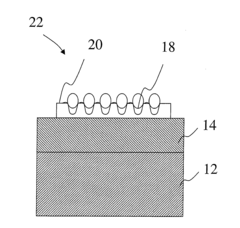
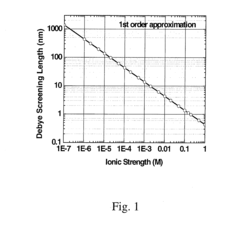
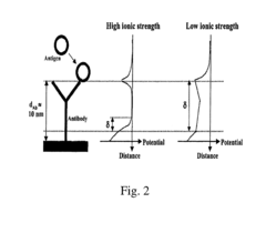
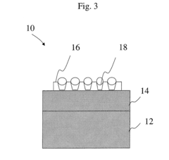
- The introduction of nanopores in the device channels of a semiconductor sensing device, which brings binding sites of antibodies or receptor molecules closer to the sensing surface, allowing the sensor to operate effectively in higher ionic strength solutions and increasing the surface-to-volume ratio for enhanced sensitivity.
Sensors and systems based on field-effect transistors, methods of preparation and devices for their operation
PatentPendingUS20230236147A1
Innovation
- A sensor with a pre-treated graphene oxide sheet and coplanar interdigitated electrodes, featuring an interfacial nanoarchitecture for non-covalent immobilization of recognition elements and a polymeric coating to enhance stability and specificity, allowing for low-volume sample analysis and multiplex diagnostics.
Regulatory Framework for Nanosensors
The regulatory framework for nanosensors is a critical aspect of their development and deployment, particularly in the context of tautomerization in interactional nanostructures. As these sensors and devices become more prevalent, governments and international bodies are working to establish comprehensive guidelines to ensure their safe and ethical use.
At the forefront of regulatory efforts is the need to address potential health and environmental risks associated with nanomaterials. Many countries have implemented specific regulations for nanomaterials, which extend to nanosensors. The European Union, for instance, has incorporated nanomaterials into its REACH (Registration, Evaluation, Authorization, and Restriction of Chemicals) regulation, requiring manufacturers to provide detailed safety information for nanomaterials used in their products.
In the United States, the Food and Drug Administration (FDA) and the Environmental Protection Agency (EPA) play crucial roles in regulating nanosensors. The FDA focuses on nanosensors used in medical applications, ensuring their safety and efficacy through rigorous testing protocols. The EPA, on the other hand, oversees environmental applications of nanosensors, particularly those used for pollution monitoring and remediation.
International standardization efforts are also underway to harmonize regulations across borders. The International Organization for Standardization (ISO) has developed several standards specific to nanotechnology, including ISO/TS 80004-1:2015, which provides a standardized vocabulary for nanotechnology applications. These standards aim to facilitate global trade and ensure consistent safety measures across different jurisdictions.
One of the key challenges in regulating nanosensors is the rapid pace of technological advancement. Regulatory bodies must strike a balance between fostering innovation and ensuring public safety. To address this, many countries have adopted adaptive regulatory frameworks that allow for periodic reviews and updates to accommodate new scientific findings and technological developments.
Privacy concerns are another significant aspect of nanosensor regulation, especially for devices capable of collecting sensitive personal or environmental data. Legislation such as the European Union's General Data Protection Regulation (GDPR) has implications for nanosensors that collect and process personal information, requiring manufacturers to implement robust data protection measures.
As the field of tautomerization in interactional nanostructures continues to evolve, it is likely that regulatory frameworks will need to adapt further. This may include the development of specific guidelines for sensors that utilize tautomeric shifts, addressing unique challenges such as signal stability and environmental sensitivity. Collaborative efforts between researchers, industry stakeholders, and regulatory bodies will be essential in crafting effective and balanced regulations that promote innovation while safeguarding public interests.
Environmental Impact of Tautomeric Nanostructures
The environmental impact of tautomeric nanostructures is a critical consideration in the development and application of these advanced materials. As tautomerization plays a crucial role in the functionality of interactional nanostructures for sensors and devices, it is essential to evaluate their potential effects on the environment throughout their lifecycle.
Tautomeric nanostructures, due to their unique properties and molecular switching capabilities, have the potential to interact with various environmental components. These interactions can occur during manufacturing, use, and disposal phases, potentially affecting air, water, and soil quality.
During the production of tautomeric nanostructures, the synthesis processes may involve the use of solvents, catalysts, and other chemicals. The release of these substances into the environment, if not properly managed, could lead to air and water pollution. Additionally, the energy consumption associated with manufacturing processes contributes to the overall carbon footprint of these materials.
In their application as sensors and devices, tautomeric nanostructures may come into direct contact with the environment. The potential for leaching or degradation of these materials over time could result in the release of nanoparticles or their byproducts into ecosystems. This raises concerns about bioaccumulation and potential toxicity to aquatic and terrestrial organisms.
The disposal of devices containing tautomeric nanostructures presents another environmental challenge. Improper disposal methods may lead to the accumulation of these materials in landfills or their release into water bodies. The long-term stability and degradation pathways of tautomeric nanostructures in the environment are areas that require further research to fully understand their ecological impact.
On the positive side, the use of tautomeric nanostructures in sensors and devices can contribute to environmental monitoring and protection. These advanced materials enable the development of highly sensitive and selective sensors for detecting pollutants, toxins, and other environmental hazards. This capability can lead to more effective environmental management and remediation strategies.
Furthermore, the molecular switching properties of tautomeric nanostructures offer potential energy-saving benefits in device applications. By enabling more efficient and responsive systems, these materials could contribute to reducing overall energy consumption and associated environmental impacts.
To mitigate potential negative environmental effects, it is crucial to adopt green chemistry principles in the design and synthesis of tautomeric nanostructures. This approach includes developing eco-friendly production methods, minimizing the use of harmful substances, and optimizing material efficiency to reduce waste.
In conclusion, while tautomeric nanostructures offer significant technological advancements, their environmental impact must be carefully considered and managed. Ongoing research into their lifecycle analysis, ecotoxicology, and sustainable production methods is essential to ensure that the benefits of these materials are realized without compromising environmental integrity.
Unlock deeper insights with Patsnap Eureka Quick Research — get a full tech report to explore trends and direct your research. Try now!
Generate Your Research Report Instantly with AI Agent
Supercharge your innovation with Patsnap Eureka AI Agent Platform!