

Thin flim transistor substrate and manufacturing method thereof
a technology of thin film transistors and manufacturing methods, which is applied in the direction of instruments, semiconductor devices, electrical devices, etc., can solve the problems of increasing the entire processing time and manufacturing cost, reducing the driving margin, and the thickness of the transistor may become non-uniform, so as to increase the driving margin and facilitate the manufacturing process. , the effect of large contact area
Patent Information
- Authority / Receiving Office
- US · United States
- Patent Type
- Applications(United States)
- Current Assignee / Owner
- Publication Date
- 2012-01-05
Smart Images
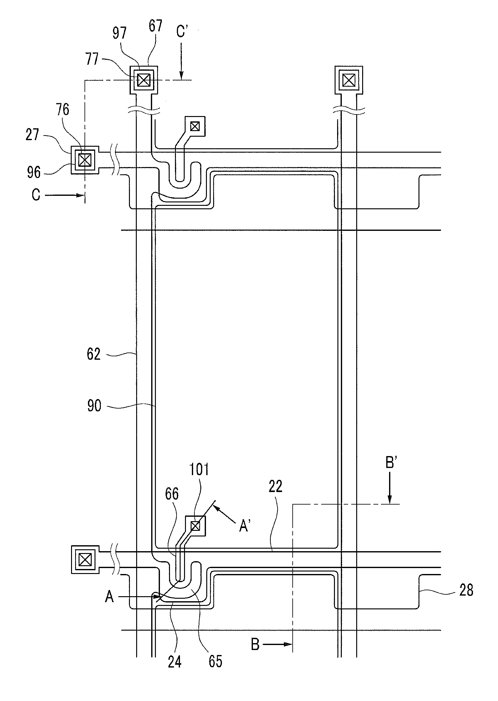
Figure 1 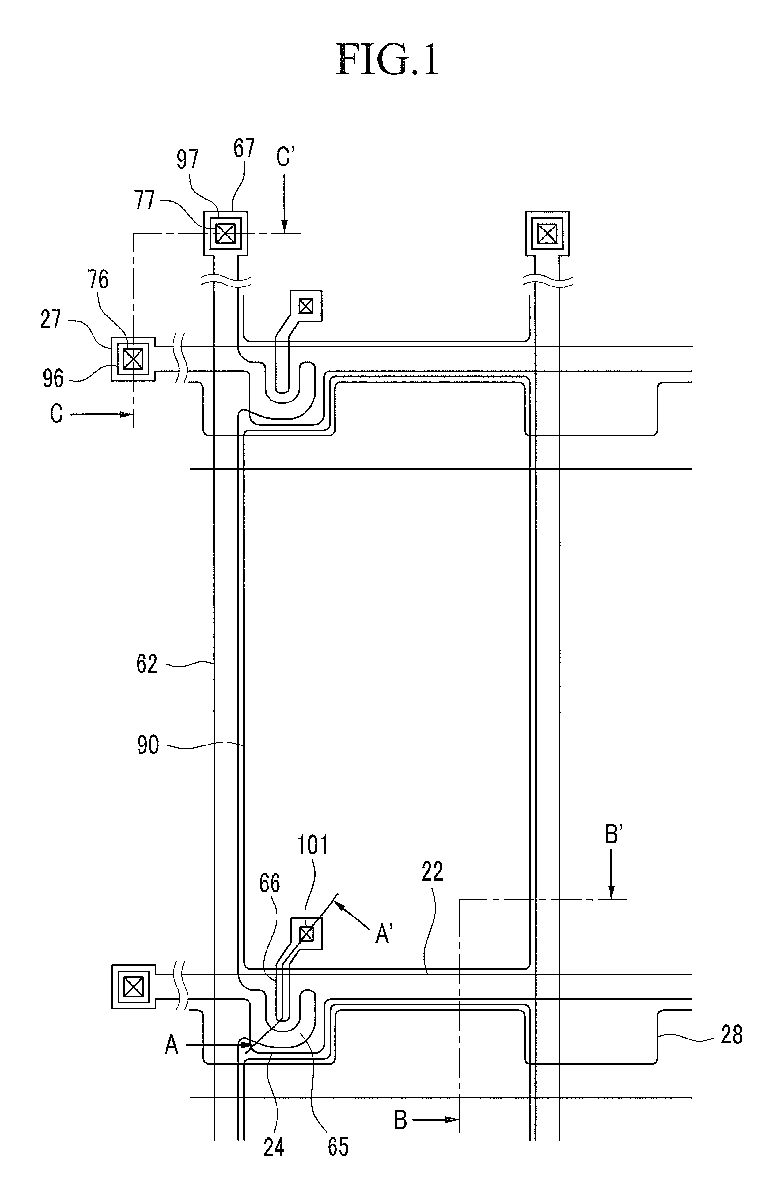
Figure 2 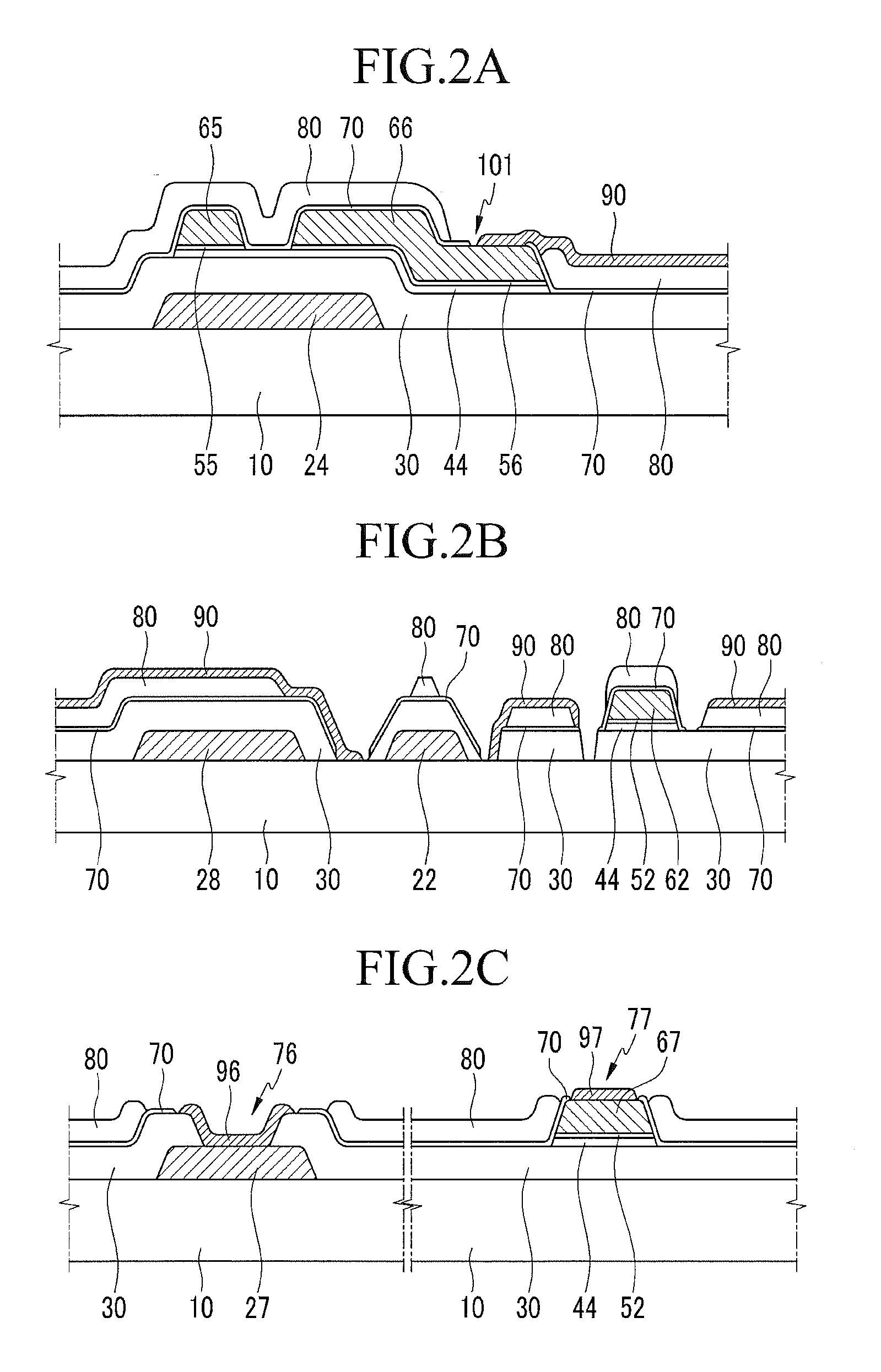
Figure 3
Abstract
Description
CROSS REFERENCE TO RELATED APPLICATIONS
[0001] This application is a divisional of U.S. patent application Ser. No. 12 / 429,388, filed on Apr. 24, 2009, which claims priority to Korean Patent Application No. 10-2008-0128494, filed on Dec. 17, 2008, and all the benefits accruing therefrom under 35 U.S.C. §119, the contents of which in its entirety are herein incorporated by reference.BACKGROUND OF THE INVENTION
[0002] 1. Field of the Invention
[0003] The present invention relates to a thin film transistor (“TFT”) array substrate and a method of fabricating the same, and more particularly, to a TFT array substrate in which a driving margin may be increased and a sufficiently large contact area between conductive materials may be provided in a contact portion, and a method of fabricating the TFT array substrate.
[0004] 2. Description of the Related Art
[0005] A liquid crystal display (LCD) includes two opposing display panels and a liquid crystal layer interposed therebetween. Each display panel ...
Examples
Embodiment Construction
[0021]Advantages and features of the present invention and methods of accomplishing the same may be understood more readily by reference to the following detailed description of preferred embodiments and the accompanying drawings. The present invention may, however, be embodied in many different forms and should not be construed as being limited to the embodiments set forth herein. Rather, these embodiments are provided so that this disclosure will be thorough and complete and will fully convey the concept of the invention to those skilled in the art, and the present invention will only be defined by the appended claims. In the drawings, the thickness of layers and regions are exaggerated or reduced for clarity.
[0022]In the following description, it will be understood that when an element or a layer is referred to as being “on” or “connected to” another element or layer, it can be directly on or directly connected to the other element or layer, or intervening layers or elements may ...