
Conductive wire frame strip, glue sealing method and glue sealing structure thereof
A lead frame strip and lead frame technology, which is applied in the fields of semiconductor devices, semiconductor/solid-state device manufacturing, semiconductor/solid-state device components, etc., can solve the problems of wasting the space of the lead frame strip 1, and it is difficult to further increase the output per unit time, etc.
Patent Information
- Authority / Receiving Office
- CN · China
- Patent Type
- Patents(China)
- Current Assignee / Owner
- Publication Date
- 2011-03-30
Smart Images
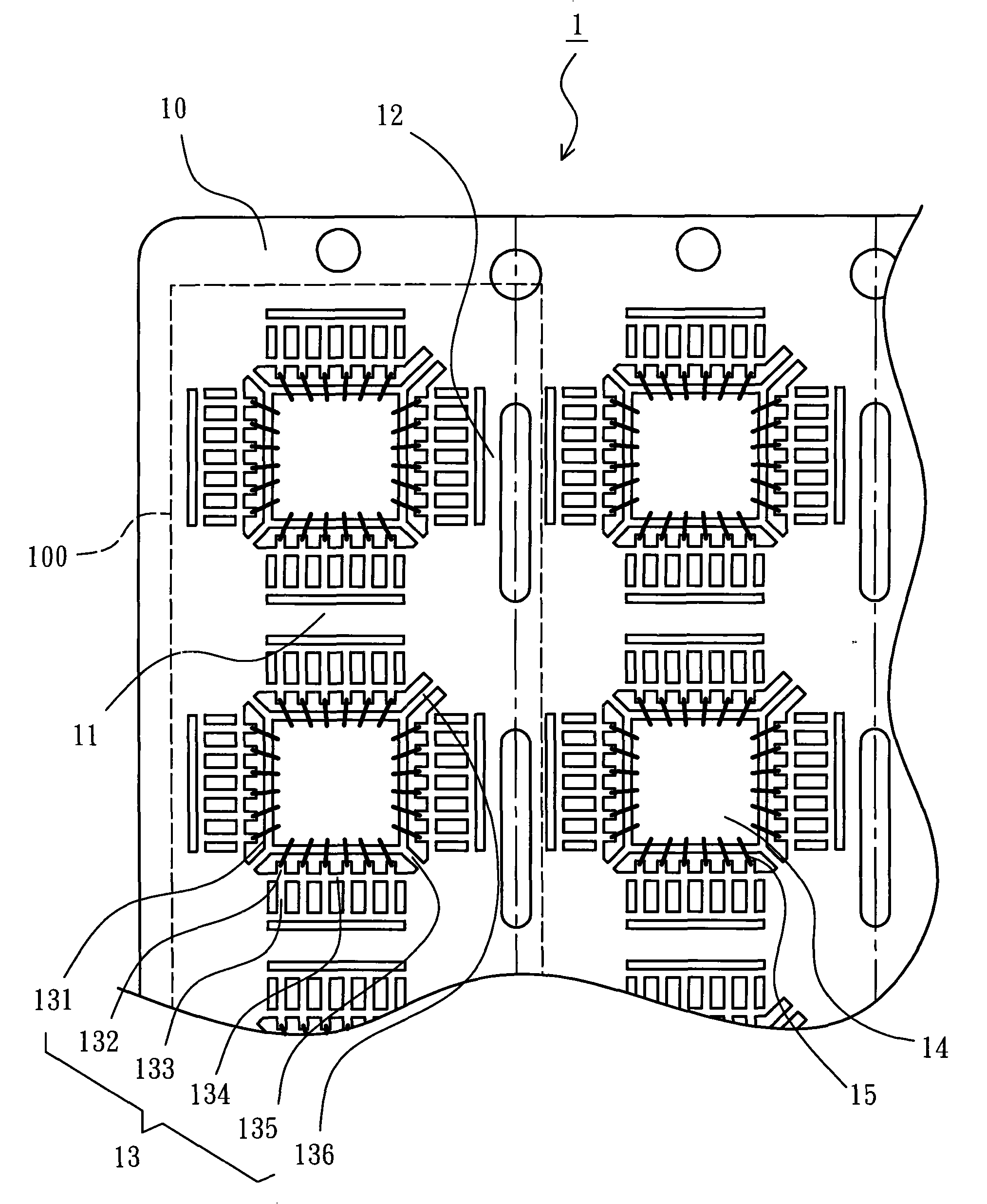
Figure 1 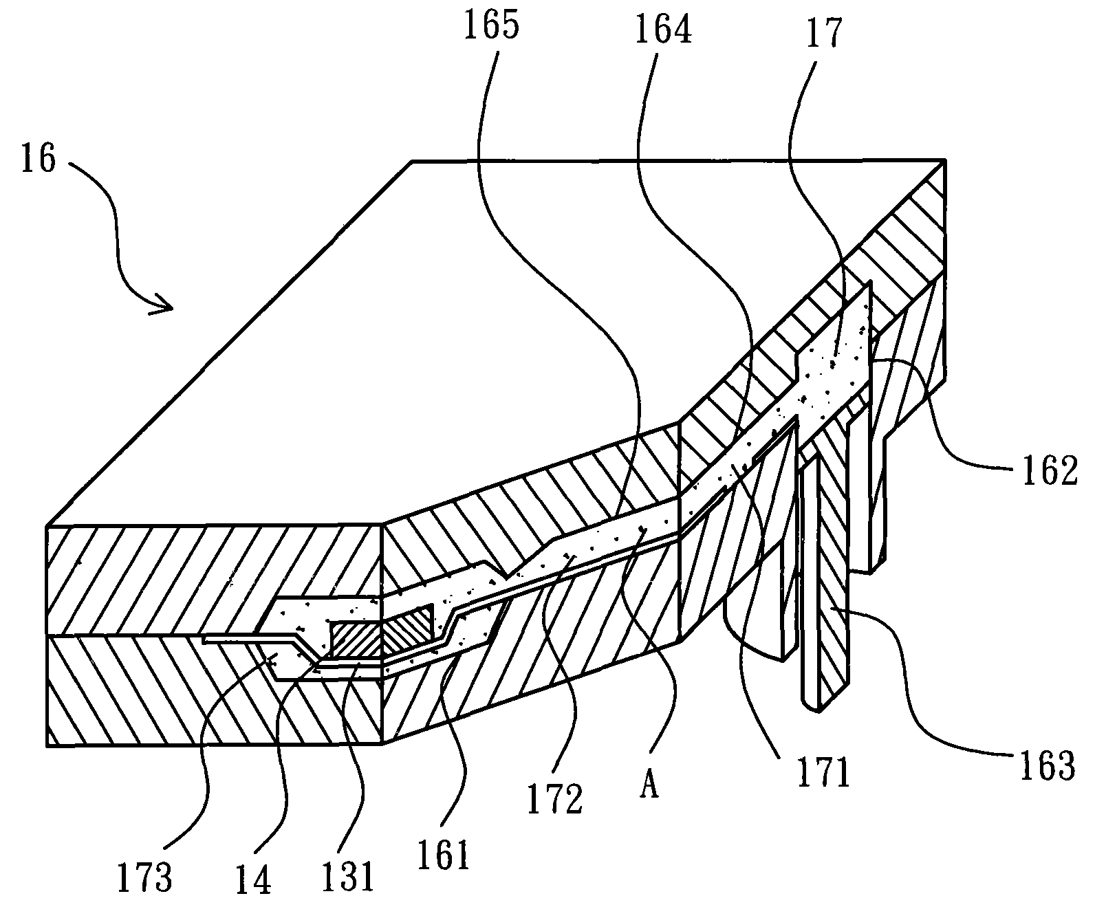
Figure 2 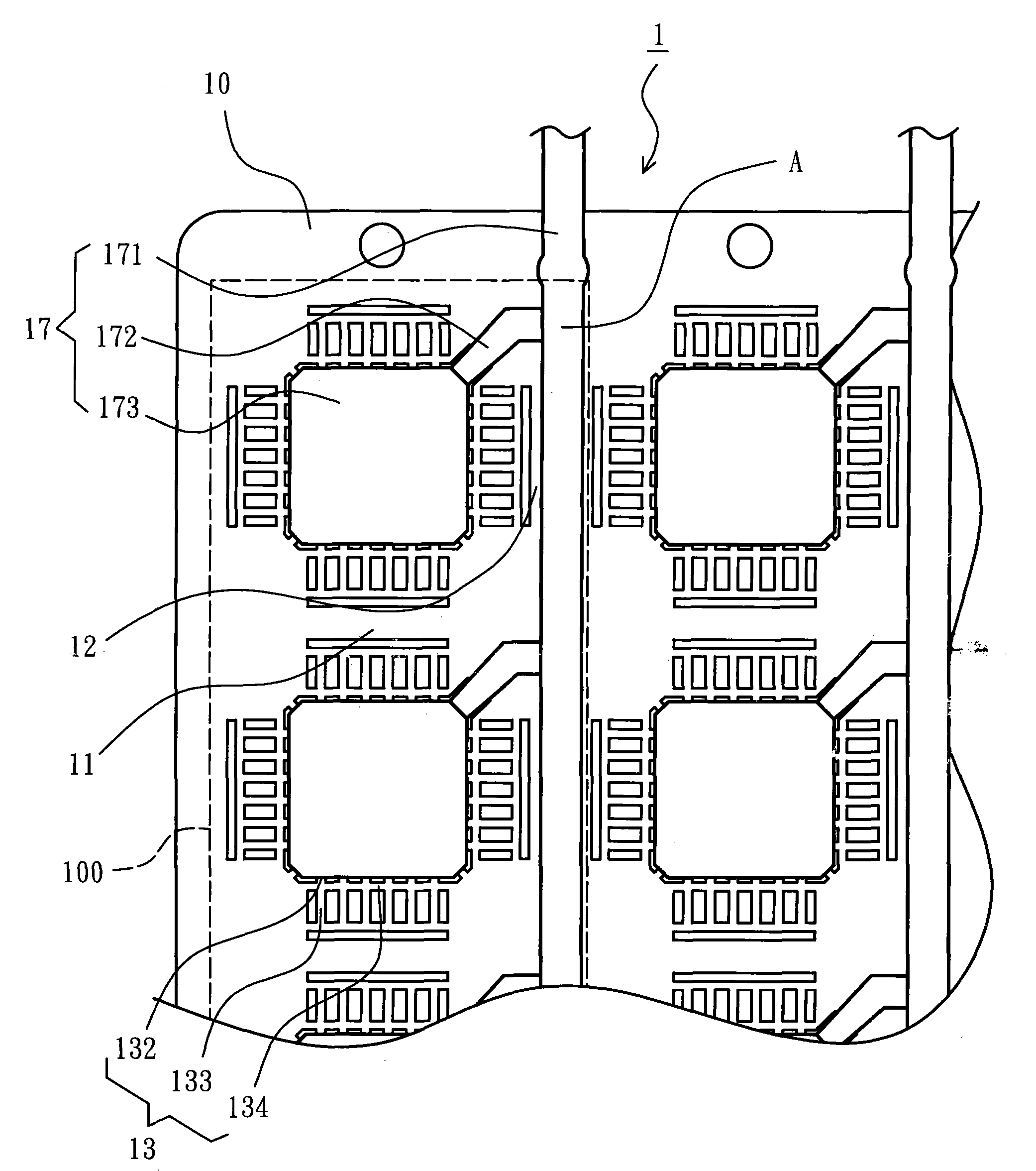
Figure 3
Abstract
Description
Technical field
[0001] The present invention relates to a lead frame strip and its sealing method and sealing structure, in particular to a lead frame strip capable of increasing the output per unit time (units per hour, UPH) and its sealing method and structure. Sealing structure.
Background technique
[0002] Nowadays, in order to meet various packaging requirements, the semiconductor packaging industry has gradually developed various types of packaging structures. Among them, silicon chips (chips) cut from semiconductor silicon wafers (wafers) are usually firstly processed by wire bonding. ) or bumping (bumping) and other appropriate methods to select and fix on the leadframe (leadframe) or substrate (substrate), and then use the encapsulation gel to encapsulate and protect the silicon chip, so that the basic structure of a semiconductor package structure can be completed. Common package structures with lead frames include small outline package (SOP), small outline J...
Examples
Embodiment Construction
[0024] In order to make the above-mentioned purposes, features and advantages of the present invention more obvious and understandable, the preferred embodiments of the present invention will be specifically cited below, together with the accompanying drawings, for a detailed description as follows:
[0025] Please refer to Figure 2A , 2BAs shown in and 2C, the lead frame bar and its sealing method and sealing structure of the preferred embodiment of the present invention are mainly used in the manufacture of semiconductor packaging products with four rows of lead frames, for example, in the manufacture of square flat packages (quad flat package, QFP), square flat non-leaded package (quad flat non-leaded package, QFN) or other similar packaging products, but can also be used to manufacture semiconductor packaging products with double-row lead frames, such as Small Outline Package (SOP), Small Outline J-Lead Package (SOJ), Small Outline Transistor Package (SOT), Small Outline...