
Near-surface defect recognition method based on ultrasonic TOFD
A defect identification, near-surface technology, applied in the field of surface and near-surface defect identification, can solve the problems of insensitivity, time-consuming, damage to near-surface defect signals, etc., to achieve the effect of simple detection process and short time-consuming
Patent Information
- Authority / Receiving Office
- CN · China
- Current Assignee / Owner
- Publication Date
- 2010-09-22
- Estimated Expiration
- Not applicable · inactive patent
Smart Images
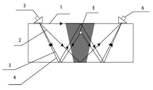
Figure 1 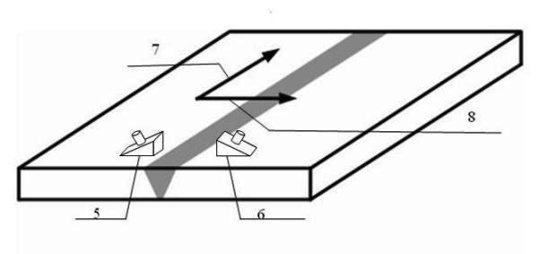
Figure 2 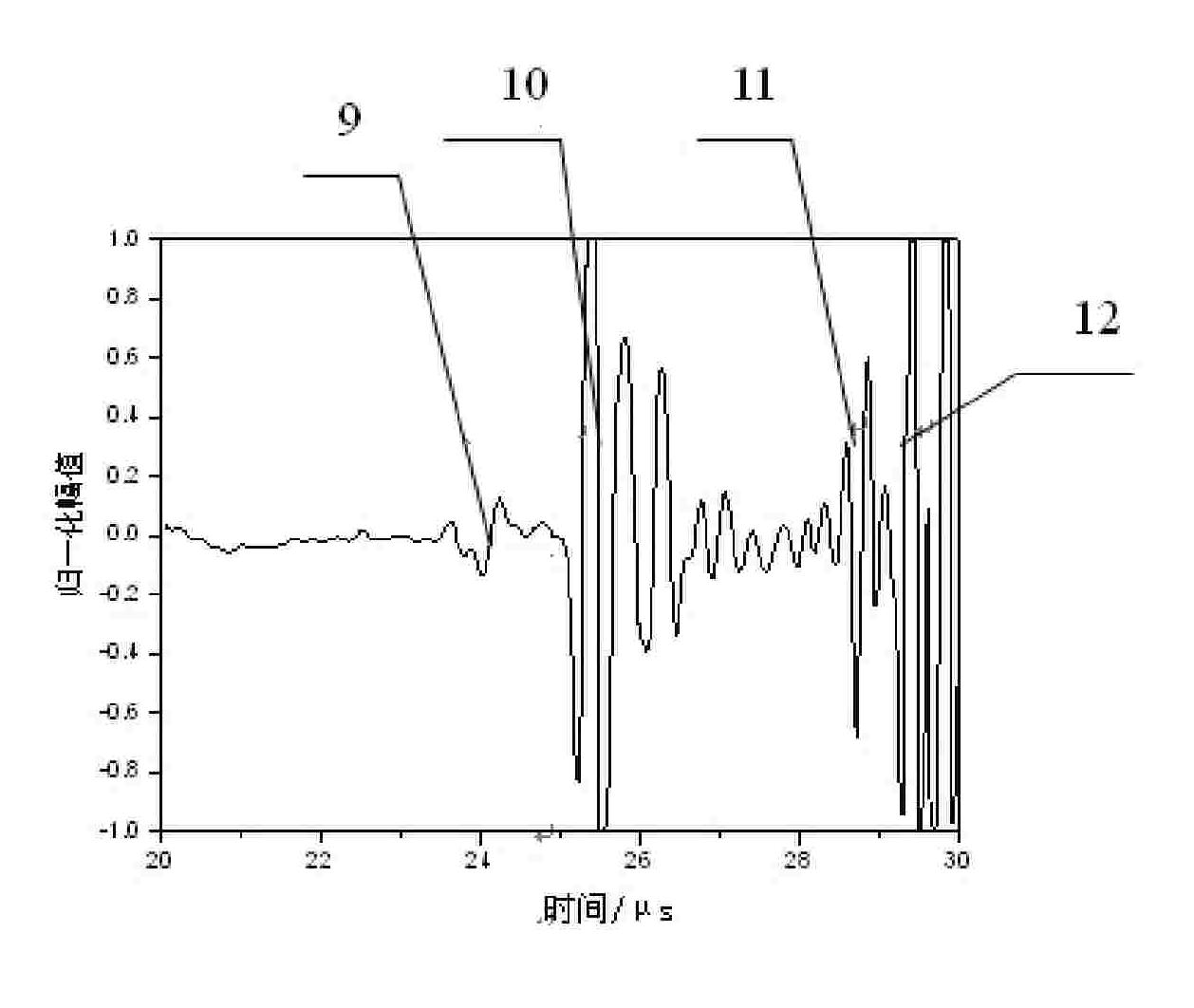
Figure 3
Abstract
Description
technical field
[0001] The invention relates to the field of ultrasonic non-destructive testing, in particular to an identification technology for surface and near-surface defects based on ultrasonic TOFD method. Background technique
[0002] Ultrasonic time-of-flight diffraction method, referred to as ultrasonic TOFD (Time of Flight Diffraction) method, is a non-destructive testing method based on receiving the diffraction signal at the end of the defect to locate and quantitatively measure the defect. It is suitable for the detection of large-thickness weld structural defects. At the same time, the ultrasonic TOFD method has the technical problem of being insensitive to near-surface defects and shallow surface opening defects. In order to solve this problem, academic paper 1: Zhang Rui et al., Ultrasonic Diffraction-Echo Transit Time Method In-Situ Quantitative Nondestructive Estimation of Weld Cracks, Chinese Journal of Mechanical Engineering, 2000, 36(5): 54~57, proposed...
Examples
specific Embodiment approach 1
[0017] Specific implementation mode one: combine figure 1 and figure 2 To illustrate this embodiment, a method for identifying near-surface defects based on ultrasonic TOFD described in this embodiment, its specific steps are:
[0018] Step 1: According to the thickness of the detected object and the refraction angle of the probe, adjust the distance between the transmitting probe 5 and the receiving probe 6, perform A-scan on the detected object, and obtain an A-scan signal;
[0019] Step 2: According to the A-scan signal obtained in Step 1, perform D-scan on the object to be detected to obtain a D-scan image;
[0020] Step 3: According to the A-scan signal obtained in Step 1, B-scan the object to be detected to obtain a B-scan image;
[0021] Step 4: According to the D-scan image obtained in step 2 and the B-scan image obtained in step 3, perform positioning measurement on the defect in the tested object, and obtain the length and burial depth of the defect in the detecte...
specific Embodiment approach 2
[0029] Specific implementation mode two: combination image 3 , Figure 4 and Figure 5 Describe this implementation mode, this implementation mode is a specific example of implementation mode 1:
[0030]In this embodiment, the artificial defect in the aluminum alloy plate is used as the detection object, the thickness of the aluminum alloy plate is 20.0 mm, the buried depth of the end of the artificial defect in the aluminum alloy plate is 2.92 mm, and the length of the artificial defect is It is a 15.0mm bottom open straight groove; the detection process is: the longitudinal wave refraction angle of the transmitting probe 5 and the receiving probe 6 in the aluminum alloy plate is 60°, and the distance between the transmitting probe 5 and the receiving probe 6 is adjusted to 110mm. Perform A-scan on the aluminum alloy plate to obtain the A-scan signal, see image 3 , according to the obtained A-scan signal, D-scan the aluminum alloy plate, mark the scanning center line on ...