
Device and method for testing performance degradation caused by transistor lattice deformation
The technology of a testing device and testing method, which is applied in the field of microelectronics, can solve problems such as inaccurate calculation of transistor lattice deformation, uneven stress on transistors, uneven stress on chips, etc., to overcome the difficulties of chip bending test methods, The effect of overcoming the limited range of mechanical stress and improving the range of mechanical stress
Patent Information
- Authority / Receiving Office
- CN · China
- Patent Type
- Patents(China)
- Current Assignee / Owner
- Publication Date
- 2015-05-20
Smart Images
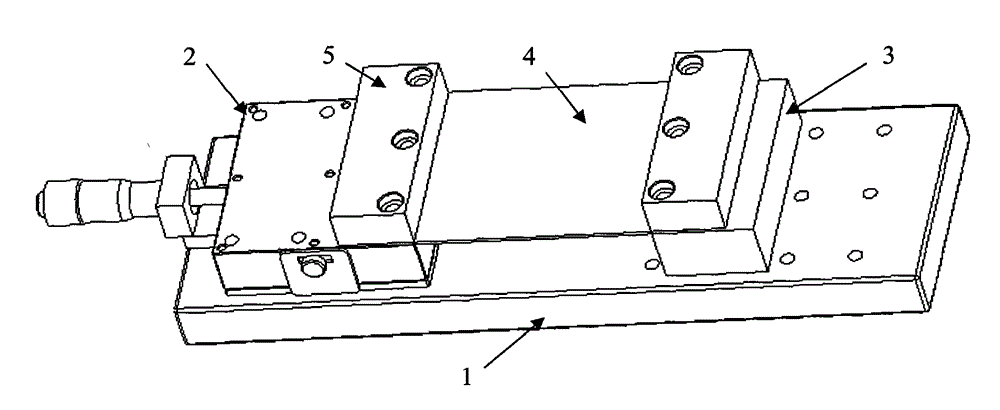
Figure 1 
Figure 2 
Figure 3
Abstract
Description
technical field
[0001] The invention belongs to the technical field of microelectronics, and further relates to a testing device and a method for performance degradation caused by lattice deformation of transistors in the technical field of semiconductor testing. The invention can be used for gallium nitride (Gallium Nitride, GaN) High Electron Mobility Transistors (High Electron Mobility Transistors, HEMTs) and other semiconductor transistor lattice deformation to cause performance degradation test, provide for the influence of transistor lattice deformation on transistor performance A more intuitive and convenient analysis method was developed. Background technique
[0002] During the working process of transistors, the generation of lattice deformation will lead to the degradation of transistor performance. This effect is more pronounced for gallium nitride high electron mobility transistors and other semiconductor devices with piezoelectric effect. Therefore, it is ver...
Examples
Embodiment Construction
[0035] Refer to attached figure 1 , a test device for performance degradation caused by transistor lattice deformation, including five parts: 1 is a base, 2 is a precision displacement platform, 3 is a spacer, 4 is a carrier, and 5 is a pressing block. in,
[0036]The cuboid base 1 is located at the bottom of the device, and one end is provided with two rows and two columns of four screw holes, which are connected with the precision displacement platform 2 on it with screws; the other end is provided with four rows and three columns of twelve screw holes. When the invention fixes the spacer 3, it can be connected with the spacer 3 on it with screws through one row of screw holes according to the specific lattice deformation test requirements. In the embodiment of the present invention, the spacer 3 is fixed on a row of screw holes on the side closest to the precise displacement platform 2 with screws.
[0037] The precision displacement platform 2 is located on the upper lef...