
P-type one-time programmable (OTP) device and manufacturing method thereof
A manufacturing method and device technology, applied in semiconductor/solid-state device manufacturing, electric solid-state devices, semiconductor devices, etc., can solve the problems of low reading current, large chip area, and small current value, so as to improve the conduction current, The effect of improved programming performance and increased coupling capacitance
Patent Information
- Authority / Receiving Office
- CN · China
- Patent Type
- Patents(China)
- Current Assignee / Owner
- Publication Date
- 2015-06-03
Smart Images
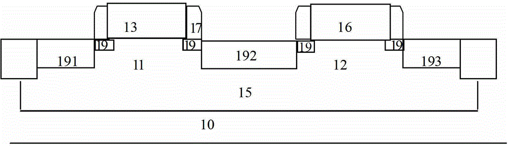
Figure 1 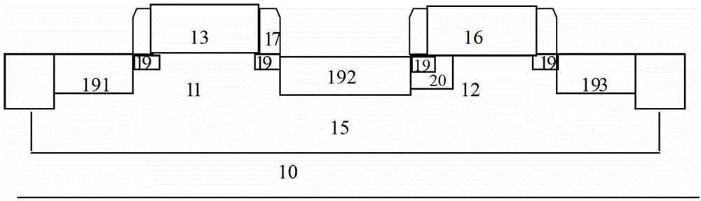
Figure 2 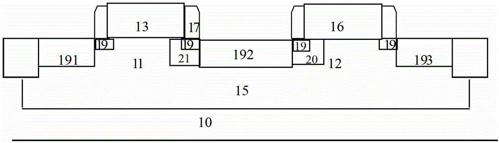
Figure 3
Abstract
Description
technical field
[0001] The invention relates to the field of manufacturing semiconductor integrated circuits, in particular to a P-type OTP device, and also relates to a method for manufacturing the P-type OTP device. Background technique
[0002] Such as figure 1 As shown, it is a schematic diagram of the structure of the existing P-type OTP device. An N-type well 15 is formed on the silicon substrate 10. It is a one-time programmable device formed by connecting two PMOS transistors 11 and 12 in series. The first PMOS transistor 11 serves as The gate transistor of the OTP device, and the second PMOS transistor 12 is used as the storage unit of the OTP device.
[0003] The source of the first PMOS transistor 11 includes a P-type diffusion region 191 and a P-type lightly doped region 19 formed in the N well, and the drain of the first PMOS transistor 11 includes a P-type diffused region 191 formed in the N well. A P-type diffusion region 192 and a P-type lightly doped regio...
Examples
Embodiment Construction
[0036] Such as figure 2 As shown, it is a schematic diagram of the structure of a P-type OTP device according to an embodiment of the present invention. An N-type well 15 is formed on a silicon substrate 10, and a one-time programmable device formed by connecting two PMOS transistors 11 and 12 in series. The first PMOS The transistor 11 is used as a pass transistor of the OTP device, and the second PMOS transistor 12 is used as a storage unit of the OTP device.
[0037] The source of the first PMOS transistor 11 includes a P-type diffusion region 191 and a P-type lightly doped region 19 formed in the N well, and the drain of the first PMOS transistor 11 includes a P-type diffused region 191 formed in the N well. A P-type diffusion region 192 and a P-type lightly doped region 19, the gate 17 of the first PMOS transistor is used as the word line of the OTP device, and the source of the first PMOS transistor 11 is used as the word line of the OTP device. Source of the OTP devic...