
Packaging structure and packaging method used for display panel
A technology for a display panel and packaging structure, which is applied in the directions of packaging, transportation and packaging, packaging of fragile items, etc., can solve problems such as affecting the optical quality of the display panel 101
Patent Information
- Authority / Receiving Office
- CN · China
- Current Assignee / Owner
- Publication Date
- 2014-03-12
- Estimated Expiration
- Not applicable · inactive patent
Smart Images
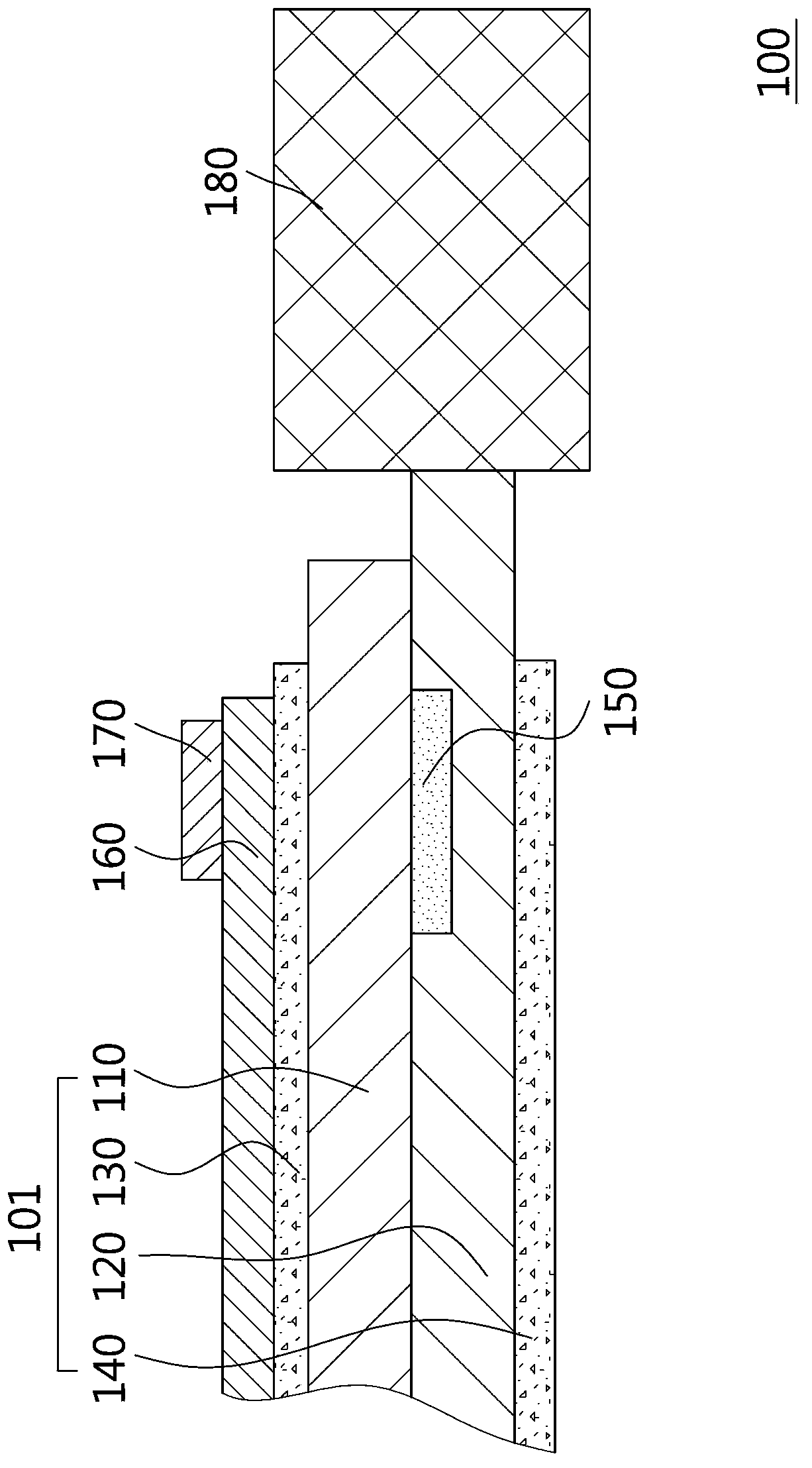
Figure 1 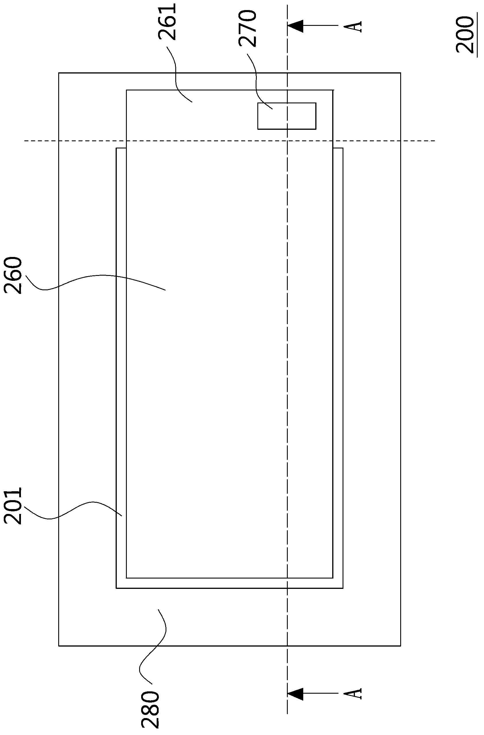
Figure 2 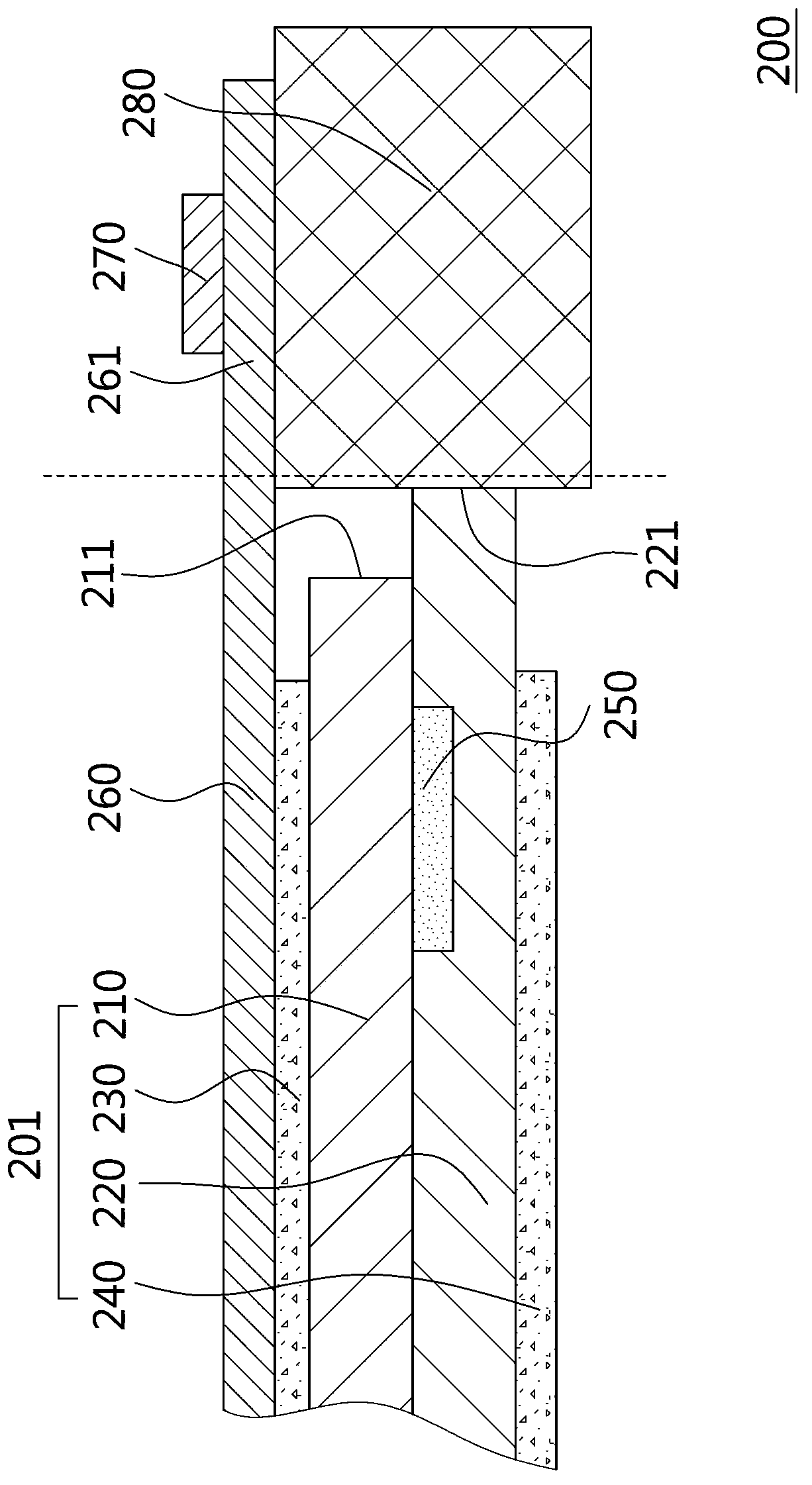
Figure 3
Abstract
Description
technical field
[0001] The present invention relates to a packaging structure and a packaging method, and in particular to a packaging structure and a packaging method for a display panel. Background technique
[0002] After the panel factory completes the display panel, it will pack the display panel, and then transport it to the display device assembly plant or assembly unit, and further integrate the display panel, backlight module, housing and other components into a display device. After the display panel is prepared, until a predetermined stage in the display device assembly process, the display panel is generally fixed with a package and attached to the display panel with a protective material to protect the display panel and prevent it from being Dirt or scratches occurred during shipping or assembly. In addition, in order to facilitate product identification and ensure a smooth assembly process, a marking unit is attached to the protective material, and the marking...
Examples
Embodiment Construction
[0036] Please also refer to figure 2 and image 3 , figure 2 Shown is a top view of a packaging structure for a display panel according to a preferred embodiment of the present invention, image 3 Shown is a schematic cross-sectional view of a packaging structure for a display panel according to a preferred embodiment of the present invention, wherein image 3 for figure 2 The section along line A-A is shown.
[0037] The packaging structure 200 is suitable for packaging the display panel 201, and the display panel 201 includes a first substrate 210 and a second substrate 220 stacked on each other. In this embodiment, a liquid crystal layer (not shown in the figure) is sandwiched between the first substrate 210 and the second substrate 220, that is, the display panel 201 adopts liquid crystal display technology, and the first substrate 210 has a color filter (color filter, CF), the second substrate 220 has a thin-film transistor (thin-film transistor, TFT), but not lim...