
Layered structure, switching element, magnetic device, and method for manufacturing layered structure
A technology of switching elements and manufacturing methods, applied in semiconductor/solid-state device manufacturing, electrical components, electric solid-state devices, etc., can solve problems such as difficulty in magnetization orientation, achieve power saving, easy control, and increase recording density.
Patent Information
- Authority / Receiving Office
- CN · China
- Patent Type
- Applications(China)
- Current Assignee / Owner
- Publication Date
- 2016-10-26
- Estimated Expiration
- Not applicable · inactive patent
Smart Images
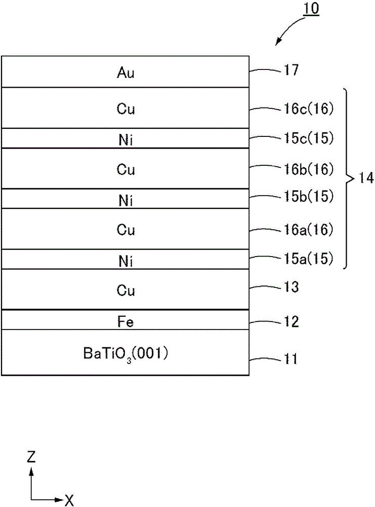
Figure 1 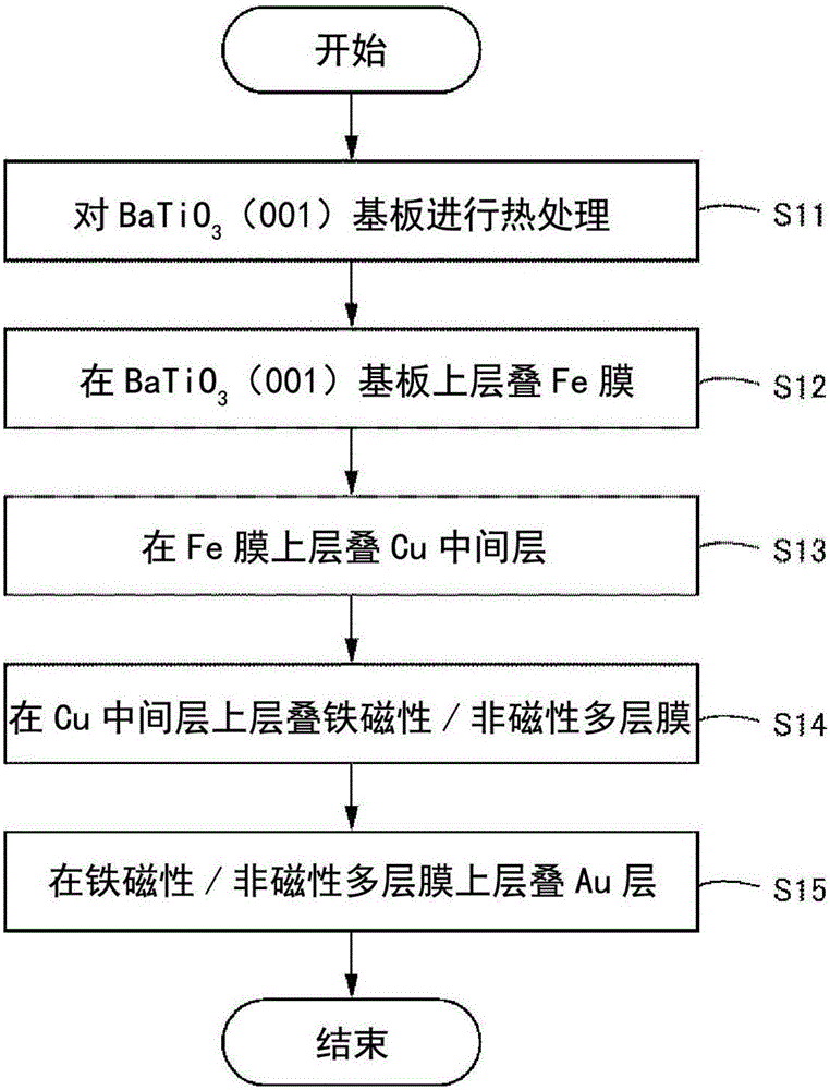
Figure 2 
Figure 3
Abstract
Description
technical field
[0001] The present invention relates to a multiferroic multiferroic structure having both ferroelectricity and ferromagnetism, a switching element including the multiferroic structure, a magnetic device including the switching element, and a method for manufacturing the multiferroic structure. This application claims priority based on Japanese Patent Application No. Japanese Patent Application No. 2014-036216 for which it applied in Japan on February 27, 2014, and takes this application in this application by reference. Background technique
[0002] Conventionally, as a method for controlling the magnetization orientation of magnetic devices such as a magnetoresistive random access memory (MRAM), a magnetic head, and a spin transistor, a method using a magnetic field has been the mainstream. In addition, in recent years, attempts have been made to realize this magnetization orientation control by using an electric current to increase the density of magnetic d...
Examples
Embodiment
[0094] Next, an example of a laminated structure according to an embodiment of the present invention will be described. The laminated structure as an example of this embodiment has a multiferroic structure of ferromagnetic / nonmagnetic multilayer film / ferroelectric, and consists of [Cu / Ni] multilayer film / Cu intermediate layer / Fe base layer / BaTiO 3 Single crystal composition. In this example, the [Cu / Ni] multilayer film with 5 cycles and BaTiO 3 The Fe base layer and the Cu intermediate layer are inserted between them, resulting in the formation of a [Cu / Ni] multilayer film on BaTiO 3 structure obtained by epitaxial growth. As a result, the ferroelectric BaTiO can be efficiently transferred through the joint interface of the [Cu / Ni] multilayer film. 3 piezoelectric strain.
[0095] For the manufacturing method of the stacked structure of this embodiment, first, using an ultra-high vacuum MBE device, a single crystal BaTiO having an in-plane-vertical dielectric multipolariza...