
display panel
A display panel and display medium layer technology, which is applied to housings with display/control units, instruments, printed circuits, etc., can solve the problem that conductive lines are difficult to meet the narrow frame design requirements, and achieve the effect of reducing the layout area
Patent Information
- Authority / Receiving Office
- CN · China
- Patent Type
- Patents(China)
- Current Assignee / Owner
- Publication Date
- 2020-03-10
Smart Images
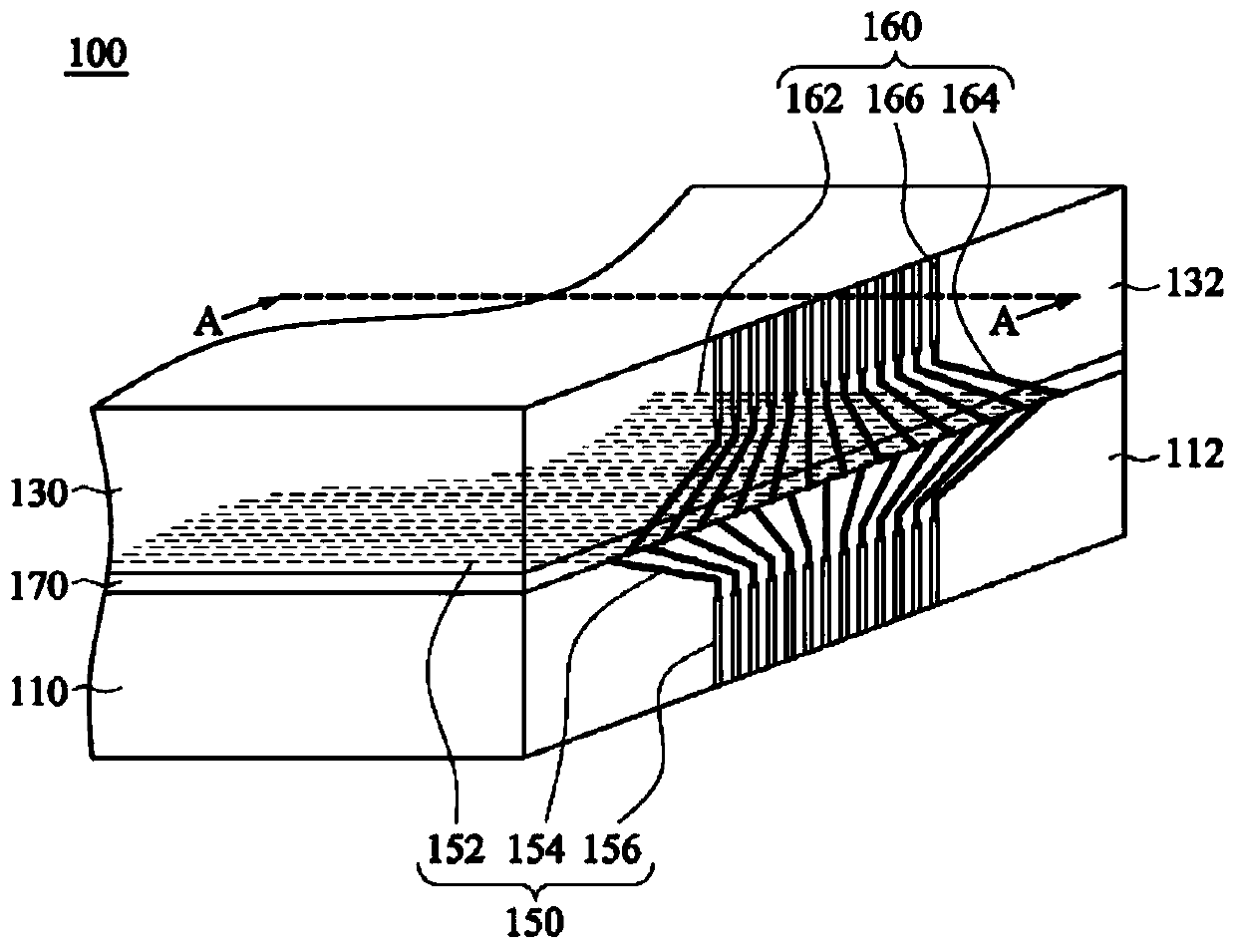
Figure 1 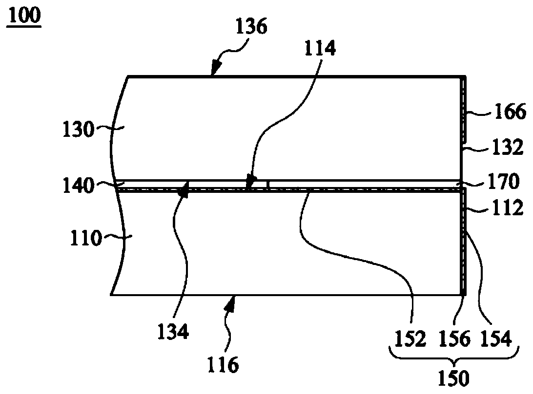
Figure 2 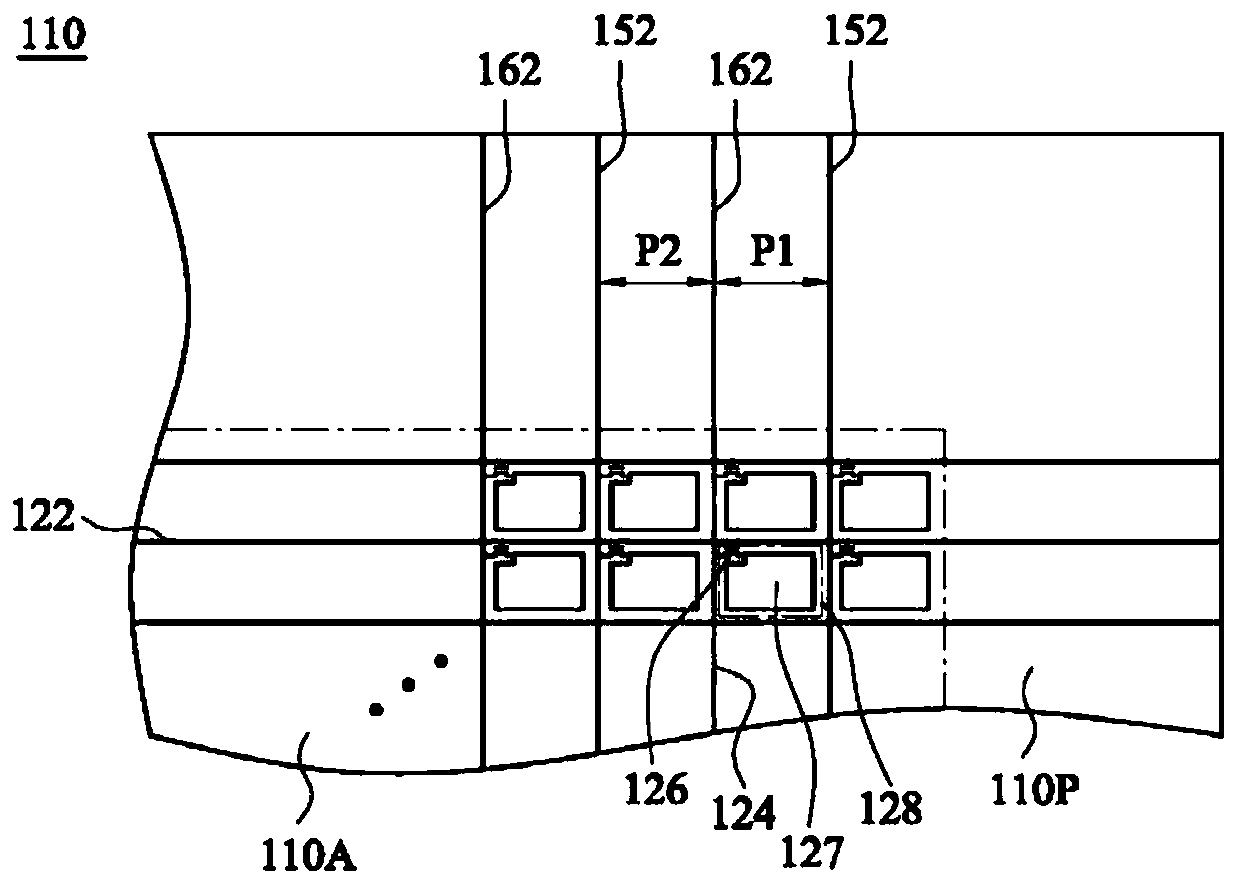
Figure 3
Abstract
Description
technical field
[0001] The present invention relates to a display panel, and in particular to a display panel with a narrow frame. Background technique
[0002] In recent years, the maturity of optoelectronic technology and semiconductor manufacturing technology has driven the development of display panel (Display Panel) technology. Existing common display panels include liquid crystal display panels, organic electroluminescence display panels, and the like. Generally speaking, a display panel has a display area, an external circuit area outside the display area, and a wiring area between the display area and the external circuit area. The display area has a plurality of pixel structures arranged in an array, and the external circuit area has circuit contacts and possible driving circuits. A plurality of wires are provided in the non-display area to electrically connect the pixel structure to the driving circuit, or to electrically connect the pixel structure to an externa...
Examples
Embodiment Construction
[0078] A number of embodiments of the present invention will be disclosed in the following figures. For the sake of clarity, many practical details will be described together in the following description. It should be understood, however, that these practical details should not be used to limit the invention. That is, in some embodiments of the present invention, these practical details are unnecessary. In addition, for the sake of simplifying the drawings, some existing conventional structures and elements will be shown in a simple and schematic manner in the drawings.
[0079] Figure 1A is a partial perspective view of a display panel 100 according to an embodiment of the present invention, Figure 1B is along Figure 1A The profile of the line segment A-A, while figure 2 yes Figure 1A A partial top view of the first substrate 110 of FIG. The display panel 100 includes a first substrate 110 , a second substrate 130 and a display medium layer 140 . The first substrate ...