
Estimation method of deterioration amount of organic el display device and organic el element
A technology of display device and degradation amount, applied in static indicators, instruments, etc., can solve problems such as image sticking, and achieve the effect of improving accuracy and suppressing image sticking.
Patent Information
- Authority / Receiving Office
- CN · China
- Patent Type
- Patents(China)
- Current Assignee / Owner
- Publication Date
- 2022-04-05
Smart Images
Figure 1 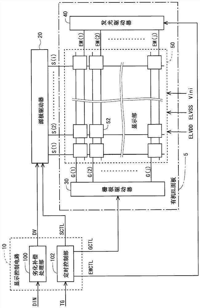
Figure 2 
Figure 3
Abstract
Description
technical field
[0001] The present invention relates to a method for estimating the deterioration amount of an organic EL display device and an organic EL element. Background technique
[0002] Conventionally, as a display element included in a display device, there are electro-optical elements whose luminance and transmittance can be controlled by an applied voltage, and electro-optic elements whose luminance and transmittance can be controlled by a flowing current. A liquid crystal display element is a representative example of an electro-optic element whose luminance and transmittance can be controlled by an applied voltage. On the other hand, an organic EL element can be cited as a representative example of an electro-optical element whose luminance and transmittance can be controlled by flowing current. The organic EL element is also called an OLED (Organic Light-Emitting Diode: Organic Light-Emitting Diode). An organic EL display device using an organic EL element, w...
Examples
Embodiment Construction
[0117] Hereinafter, one embodiment of the present invention will be described with reference to the drawings. In the following description, it is assumed that i and j are integers of 2 or more, m is an integer of 1 or more and i or less, and n is an integer of 1 or more and j or less.
[0118]
[0119] figure 2 It is a block diagram showing the overall configuration of an organic EL display device according to one embodiment of the present invention. The organic EL display device includes a display control circuit 10 , a source driver (data line drive circuit) 20 , a gate driver (scanning signal line drive circuit) 30 , a light emission driver (light emission control line drive circuit) 40 and a display portion 50 . In this embodiment, the gate driver 30 and the light emission driver 40 are formed in the organic EL panel 5 including the display unit 50 . That is, the gate driver 30 and the light emission driver 40 are singulated. However, a structure in which the gate dr...