
Photoelectric sensor and display panel
A photoelectric sensor and display panel technology, applied in the field of photoelectric sensing, can solve the problems of small photocurrent and low photoelectric conversion efficiency, and achieve the effect of increasing photocurrent, improving photoelectric conversion efficiency, and prolonging the accumulation time
Patent Information
- Authority / Receiving Office
- CN · China
- Patent Type
- Applications(China)
- Current Assignee / Owner
- Publication Date
- 2020-05-15
- Estimated Expiration
- Not applicable · inactive patent
Smart Images
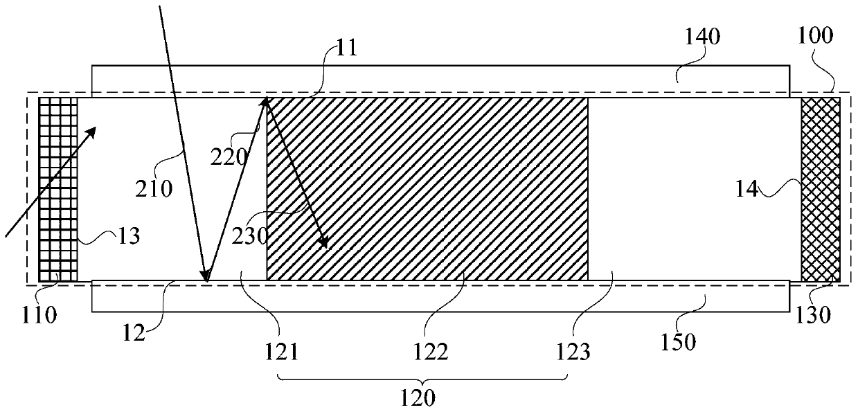
Figure 1 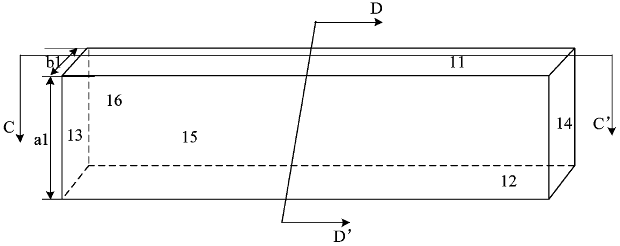
Figure 2 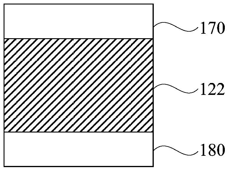
Figure 3
Abstract
Description
technical field
[0001] Embodiments of the present invention relate to the technical field of photoelectric sensing, and in particular, to a photoelectric sensor and a display panel. Background technique
[0002] As a photodetector, the photoelectric sensor can detect the light power incident on it and complete the conversion of the photoelectric signal. It is widely used in fingerprint recognition and other fields.
[0003] Existing photosensors usually include a photodiode, and the structure of the photodiode is usually a layer of intrinsic semiconductor (referred to as I) with a very low doping concentration in a PN junction, that is, a PIN photosensor.
[0004] However, existing photoelectric sensors have the problems of low photoelectric conversion efficiency and small photocurrent. Contents of the invention
[0005] The invention provides a photoelectric sensor and a display panel to improve the photoelectric conversion efficiency of the photoelectric sensor and incr...
Examples
Embodiment Construction
[0031] The present invention will be further described in detail below in conjunction with the accompanying drawings and embodiments. It should be understood that the specific embodiments described here are only used to explain the present invention, but not to limit the present invention. In addition, it should be noted that, for the convenience of description, only some structures related to the present invention are shown in the drawings but not all structures.
[0032] As mentioned in the background art, existing photoelectric sensors have the problems of low photoelectric conversion efficiency and small photocurrent. The inventor found that the reason for the above problems is that the photoelectric sensor is a device that converts light into electricity, and the longer the light stays in the photoelectric sensor, the longer the light action time on the photodiode in the photoelectric sensor is. The higher the photoelectric conversion efficiency, the larger the photocurr...