
Low-frequency low-power-consumption array substrate and manufacturing method thereof
A technology for array substrates and manufacturing methods, which is applied in the field of low-frequency and low-power array substrates and their manufacture, can solve problems such as space occupation, pixel density reduction, and liquid crystal panel resolution reduction, and achieve the effect of reducing area and ensuring pixel resolution
Patent Information
- Authority / Receiving Office
- CN · China
- Patent Type
- Applications(China)
- Current Assignee / Owner
- Publication Date
- 2021-02-12
- Estimated Expiration
- Not applicable · inactive patent
Smart Images
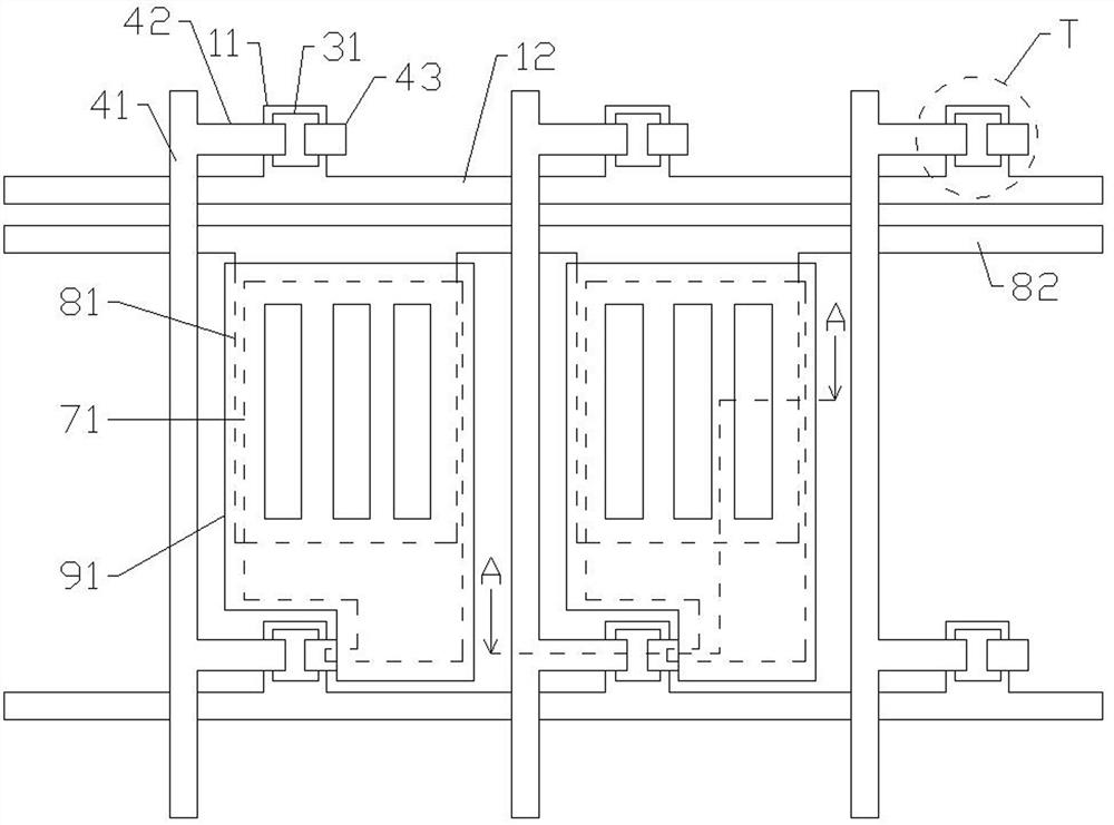
Figure 1 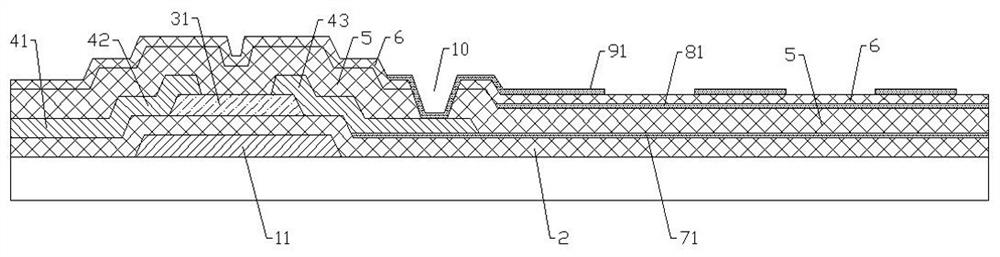
Figure 2 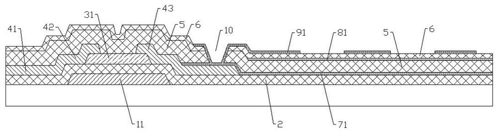
Figure 3
Abstract
Description
technical field
[0001] The invention relates to display technology, in particular to a low-frequency and low-power consumption array substrate and a manufacturing method thereof. Background technique
[0002] With the development of the panel display industry, the resolution requirements of the liquid crystal panel are getting higher and higher, and the power consumption of the liquid crystal panel is also increasing accordingly. In order to reduce power consumption without lowering the resolution, it is often used to reduce the refresh frequency of the liquid crystal panel to achieve the purpose of reducing power consumption.
[0003] In the prior art, a common electrode layer VCOM is provided on the TFT substrate of the liquid crystal panel, and the common electrode in the common electrode layer VCOM will insulate and overlap with the pixel electrodes to form a storage capacitor. The liquid crystal panel relies on the The storage capacitor is used so that the pixel electr...
Examples
Embodiment Construction
[0046] The present invention will be described in detail below in conjunction with the accompanying drawings and embodiments.
[0047] Such as Figure 1-6 As shown, a low-frequency and low-power array substrate includes a switch area and a pixel area.
[0048] The switch region includes a thin film transistor T, and the thin film transistor T includes a gate layer stacked up and down, a gate insulating layer 2, an active layer, a source drain layer, a first insulating layer 5 and a second insulating layer 6, and the gate The layer includes a gate 11 and a gate line 12 (GATE), the gate 11 is electrically connected to the gate line 12; the active layer includes a silicon island 31 on the gate insulating layer 2, the The silicon island 31 overlaps with the gate 11; the source-drain layer includes a data line 41 (SD) on the gate insulating layer 2, a source 42 on one side of the silicon island 31, a The drain 43 on the other side of the silicon island 31 is electrically connecte...