
Methods for assembling semiconductor devices in superimposed relation with adhesive material defining the distance adjacent semiconductor devices are spaced apart from one another
a technology of adhesive material and semiconductor device, which is applied in the direction of semiconductor device details, semiconductor/solid-state device details, electrical apparatus, etc., can solve the problems of wasting adhesive, reducing the actual practice of incorporation of different types of functionality into a single semiconductor device, and severely limited obtainable height of such multi-chip modules, so as to facilitate the introduction and spread of the effect of reducing the overall height of the assembly and facilitating the introduction
Patent Information
- Authority / Receiving Office
- US · United States
- Patent Type
- Applications(United States)
- Current Assignee / Owner
- Publication Date
- 2005-03-31
- Estimated Expiration
- Not applicable · inactive patent
Smart Images
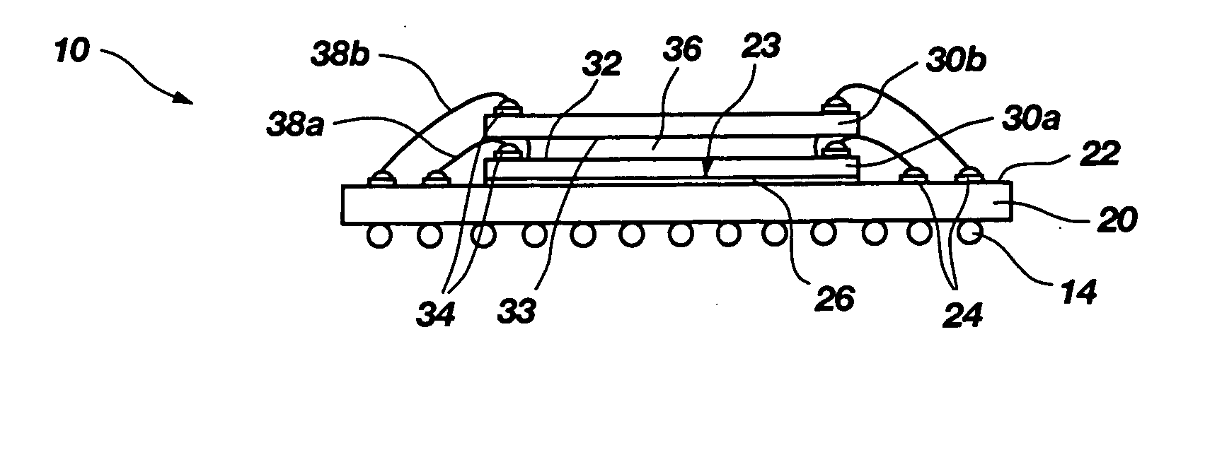
Figure 1 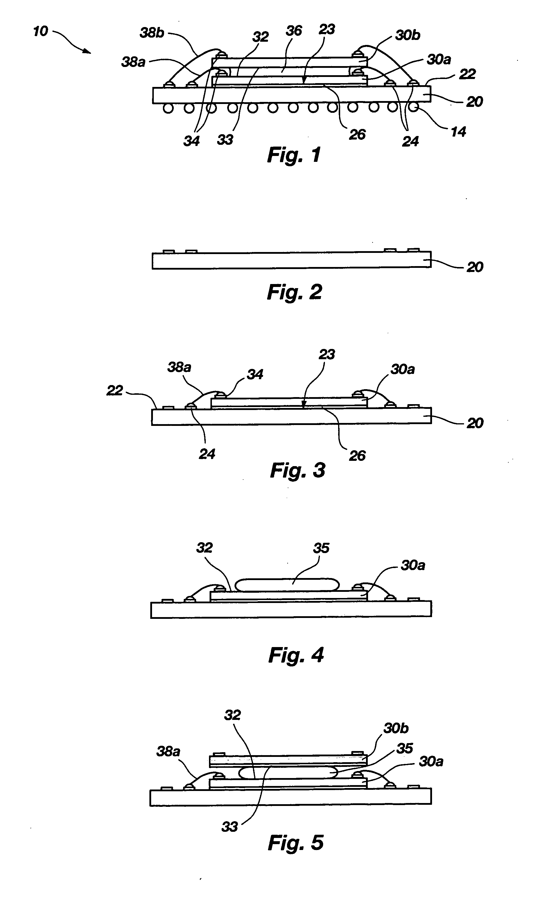
Figure 2 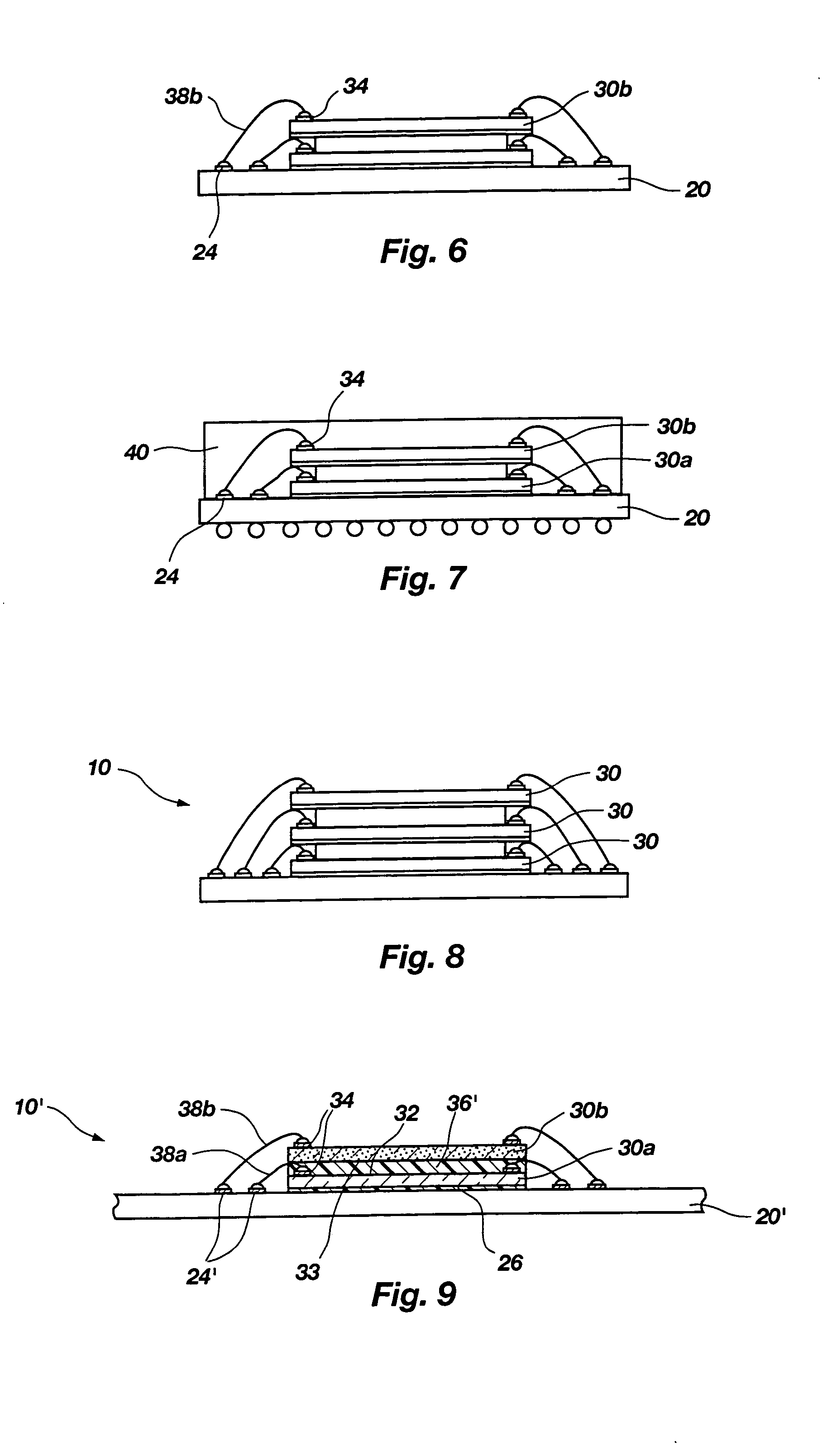
Figure 3
Abstract
Description
CROSS-REFERENCE TO RELATED APPLICATIONS
[0001] This application is a continuation of application Ser. No. 10 / 446,382, filed May 27, 2003, pending, which is a continuation of application Ser. No. 09 / 977,456, filed Oct. 15, 2001, now U.S. Pat. No. 6,569,709, issued May 27, 2003.BACKGROUND OF THE INVENTION
[0002] 1. Field of the Invention
[0003] The present invention relates generally to semiconductor device assemblies, or so-called “multi-chip modules,” and, more specifically, to multi-chip modules in which two or more semiconductor devices are stacked relative to one another. In particular, the present invention relates to stacked semiconductor device assemblies in which the upper semiconductor device of an adjacent pair of semiconductor devices at least partially overlies discrete conductive elements protruding above the lower semiconductor device of the adjacent pair and the distances between adjacent, stacked semiconductor devices are determined, at least in part, by a quantity of...
Examples
Embodiment Construction
[0041] With reference to FIG. 1, an exemplary embodiment of an assembly 10 incorporating teachings of the present invention is illustrated. As shown, assembly 10 includes a substrate 20 with two semiconductor devices 30a, 30b (collectively referred to as “semiconductor devices 30”) positioned thereover in stacked arrangement.
[0042] The depicted substrate 20 is an interposer with a number of bond pads, which are referred to herein as contact areas 24, through which electrical signals are input to or output from semiconductor devices 30 carried upon or adjacent to a surface 22 of substrate 20. Each contact area 24 corresponds to a bond pad 34 on an active surface 32 of one of the semiconductor devices 30 positioned upon substrate 20.
[0043] Of course, the use of other types of substrates, such as circuit boards, semiconductor devices, leads, and the like, in assemblies and assembly methods incorporating teachings of the present invention is also within the scope of the present invent...