
Methods for enhancing within-wafer CMP uniformity
a technology of uniformity and polishing profile, applied in the direction of grinding machines, manufacturing tools, lapping machines, etc., can solve the problems of poor lithography, window-etching or plug-formation difficulties, and the difficulty in controlling the polishing rate at different locations on the wafer surface, so as to facilitate substantially equal polishing rates and enhance the uniformity of the polishing profile of the substrate. , the effect of uniform polishing profil
Patent Information
- Authority / Receiving Office
- US · United States
- Patent Type
- Applications(United States)
- Current Assignee / Owner
- Publication Date
- 2005-04-14
- Estimated Expiration
- Not applicable · inactive patent
Smart Images
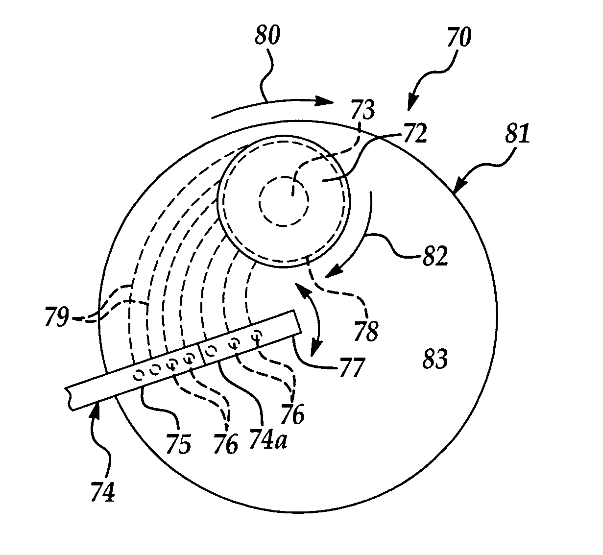
Figure 1 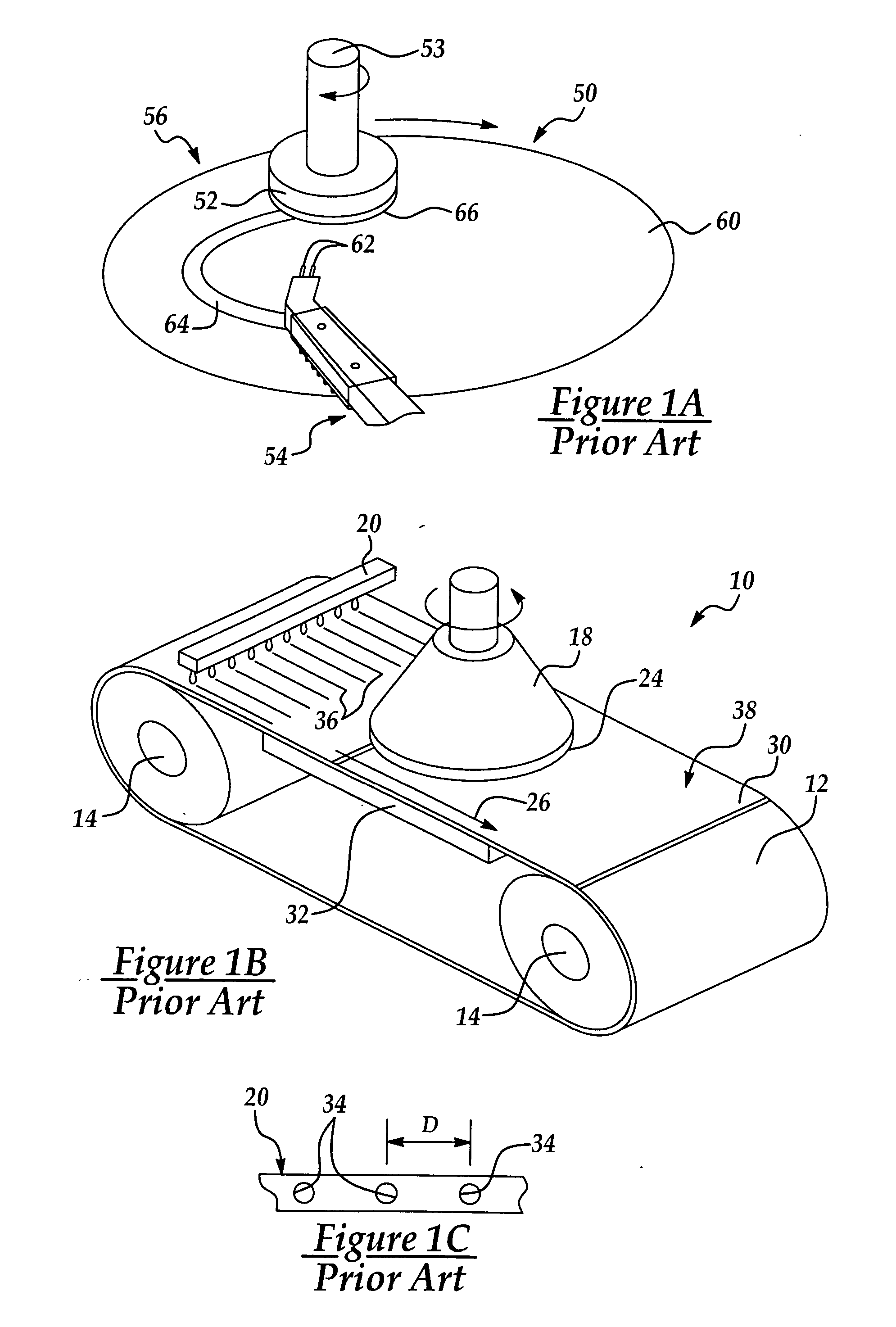
Figure 2 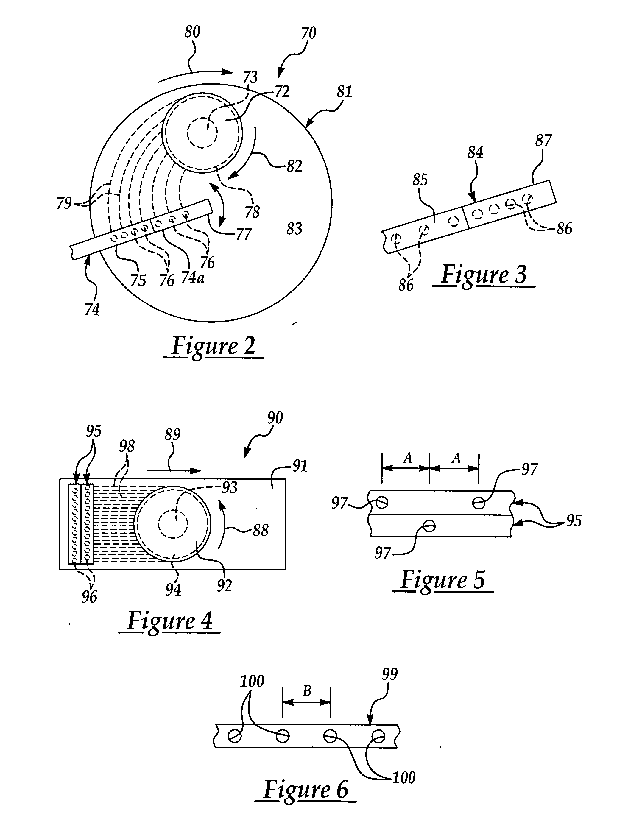
Figure 3
Abstract
Description
FIELD OF THE INVENTION
[0001] The present invention relates to chemical mechanical polishing apparatus used in the polishing of semiconductor wafers. More particularly, the present invention relates to methods for enhancing uniformity in the polishing profile of substrates during chemical mechanical polishing (CMP). BACKGROUND OF THE INVENTION
[0002] In the fabrication of semiconductor devices from a silicon wafer, a variety of semiconductor processing equipment and tools are utilized. One of these processing tools is used for polishing thin, flat semiconductor wafers to obtain a planarized surface. A planarized surface is highly desirable on a shadow trench isolation (STI) layer, inter-layer dielectric (ILD) or on an inter-metal dielectric (IMD) layer, which are frequently used in memory devices. The planarization process is important since it enables the subsequent use of a high-resolution lithographic process to fabricate the next-level circuit. The accuracy of a high resolution ...
Examples
Embodiment Construction
[0034] The present invention has particularly beneficial utility in the polishing or planarization of semiconductor wafer substrates used in the fabrication of semiconductor integrated circuits. However, the invention is not so limited in application, and while references may be made to such semiconductor wafer substrates, the present invention may be more generally applicable to polishing or planarization of substrates in a variety of mechanical and industrial applications.
[0035] Referring initially to FIGS. 2 and 3, a rotary CMP apparatus 70 in implementation of the present invention includes a circular polishing pad 81. A wafer carrier 72, typically mounted on the bottom end of a vertical shaft 73, is disposed above the upper surface 83 of the polishing pad 81, in conventional fashion. In use, a wafer 78 is mounted on the bottom surface of the wafer carrier 72, typically in conventional fashion, and the wafer carrier 72 rotates the wafer 78 against the upper surface of the polis...