
Method for inspecting insulating film for film carrier tape for mounting electronic components thereon, inspection apparatus for inspecting the insulating film, punching apparatus for punching the insulating film, and method for controlling the punching apparatus
Patent Information
- Authority / Receiving Office
- US · United States
- Current Assignee / Owner
- Publication Date
- 2005-11-03
- Estimated Expiration
- Not applicable · inactive patent
Smart Images
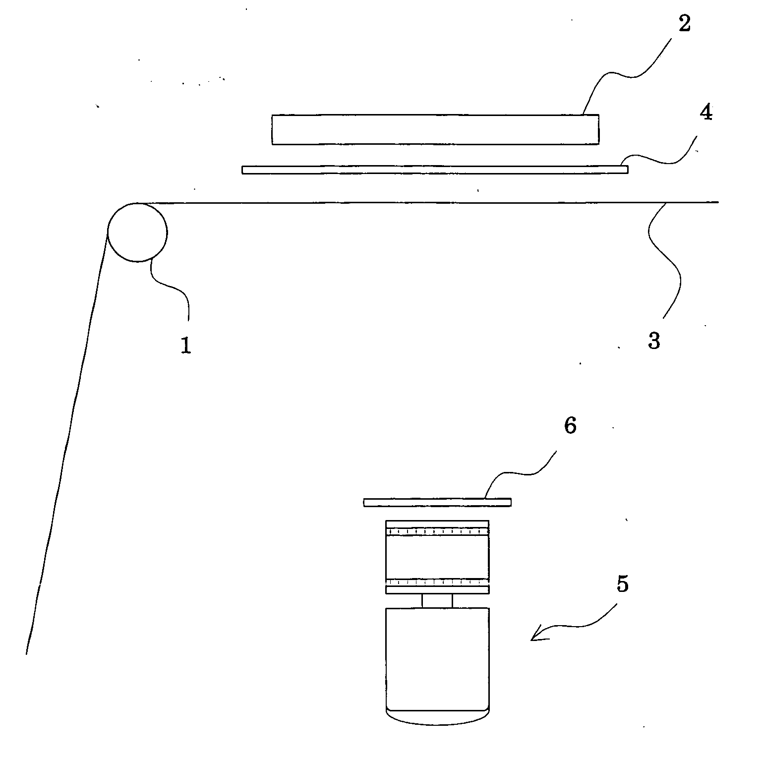
Figure 1 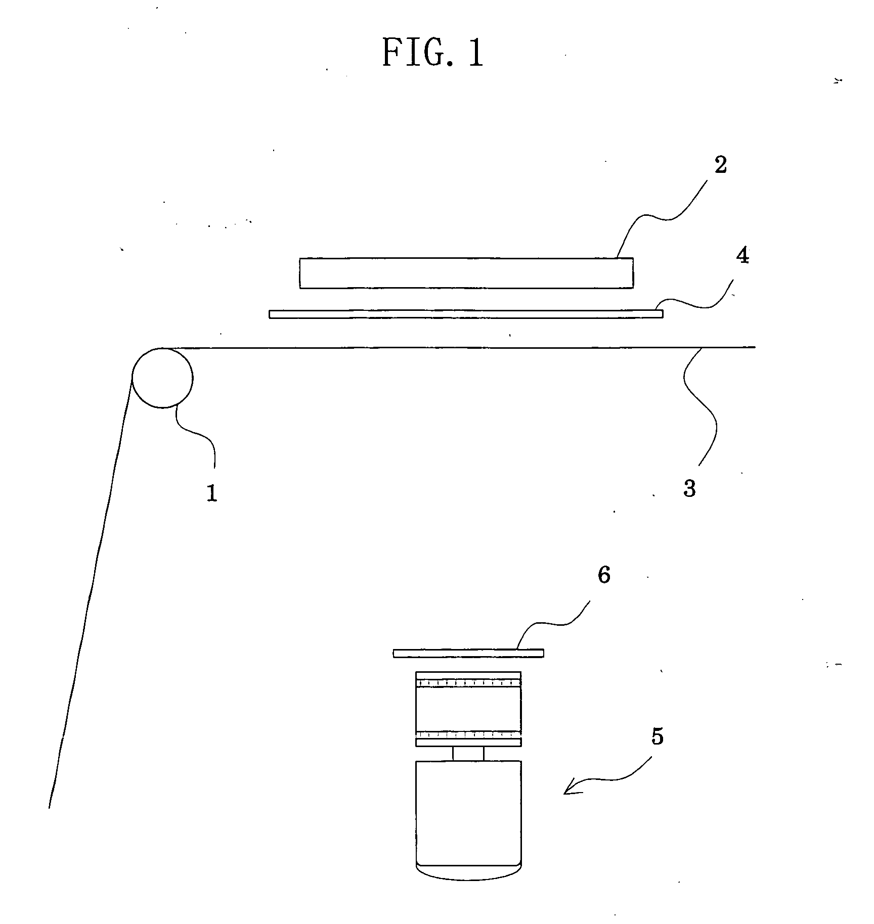
Figure 2 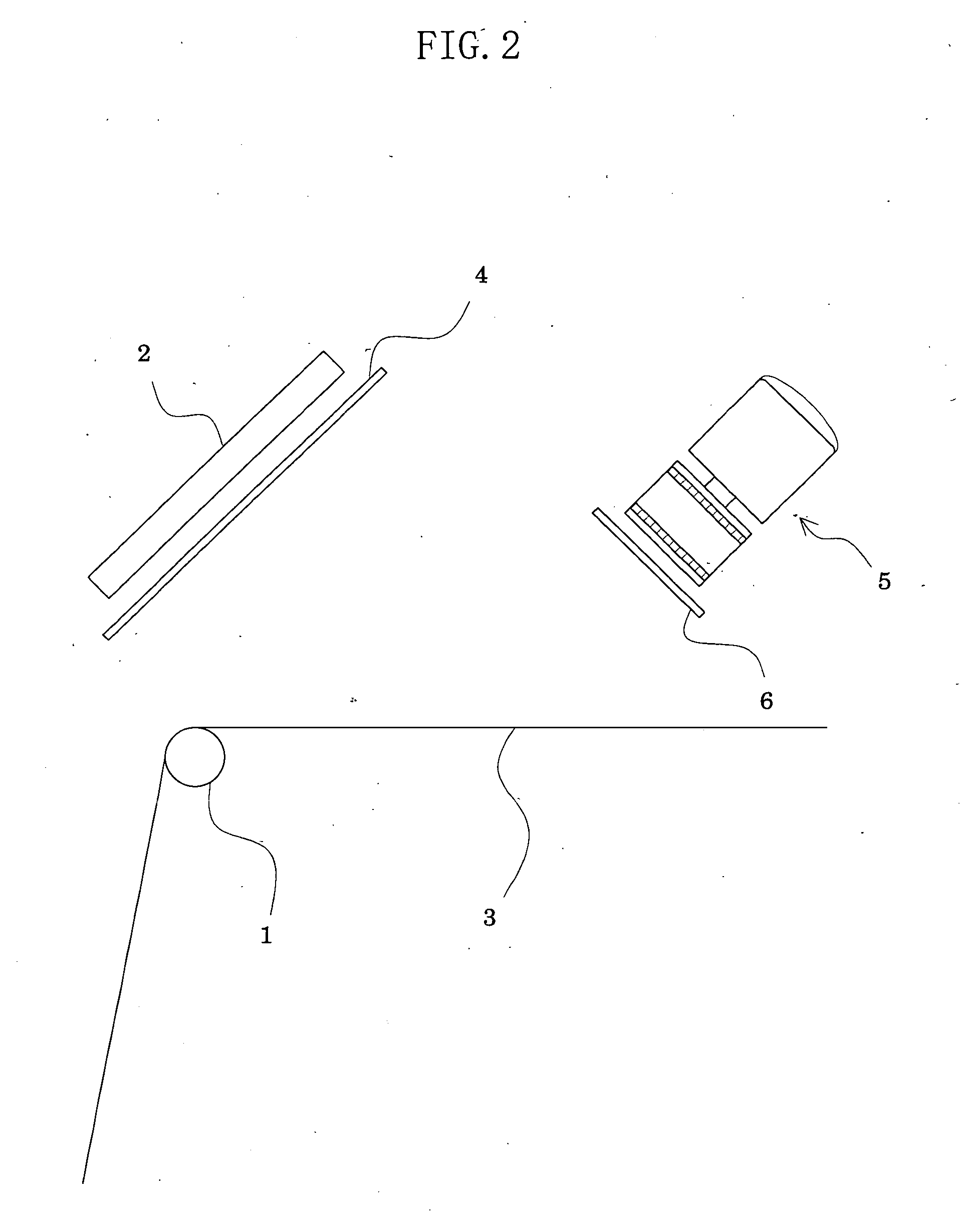
Figure 3
Abstract
Description
BACKGROUND OF THE INVENTION
[0001] 1. Field of the Invention
[0002] The present invention relates to a method for inspecting insulating film (in the form of a long tape or sheet) for use in production of a film carrier tape for mounting electronic components thereon, such as a TAB (tape automated bonding) tape, a COF (chip on film) tape, a CSP (chip size package) tape, a BGA (ball grid array) tape, a μ-BGA (μ-ball grid array) tape, a FC (flip chip) tape, a QFP (quad flat package) tape, or an FPC (flexible printed circuit) tape (hereinafter such tapes are collectively referred to simply as film carrier tapes); to an inspection apparatus for detecting defects of an insulating film for film carrier tape for mounting electronic components thereon (hereinafter referred to simply as “an insulating film for film carrier tape ”) ; to a punching apparatus for punching an insulating film for film carrier tape; and to a method for controlling a punching apparatus for punching an insulating fil...
Examples
Embodiment Construction
[0049] With reference to the attached drawings, preferred embodiments of the method for inspecting an insulating film for film carrier tape, the inspection apparatus, the punching apparatus for punching an insulating film for film carrier tape, and the method for controlling the punching apparatus according to the present invention will next be described in detail.
[0050]FIG. 1 shows an inspection apparatus for detecting defects present inside or on the top surface or the bottom surface of an insulating film 3 for film carrier tape, the apparatus comprising: a conveying means 1 (e.g. a roller) for conveying the insulating film 3 for film carrier tape; a light source 2 (e.g., an LED) for emitting parallel rays; a first polarizing filter 4 disposed between the light source 2 and a conveying path for the insulating film 3 for film carrier tape; an image pickup device 5 (e.g., a CCD camera); a second polarizing filter 6 disposed between the image pickup device 5 and the conveying path f...