
Static random access memory
a random access memory and random access technology, applied in static storage, digital storage, instruments, etc., can solve the problems of low-performance mos transistors in latches, low-performance devices for fast flipping during write operation, and failure of flipping, so as to reduce the operation cycle time and fast access time , the effect of low power consumption
Patent Information
- Authority / Receiving Office
- US · United States
- Patent Type
- Applications(United States)
- Current Assignee / Owner
- Publication Date
- 2007-09-20
- Estimated Expiration
- Not applicable · inactive patent
Smart Images
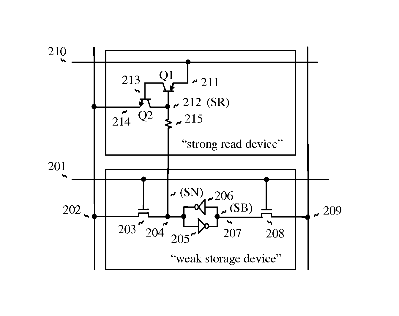
Figure 1 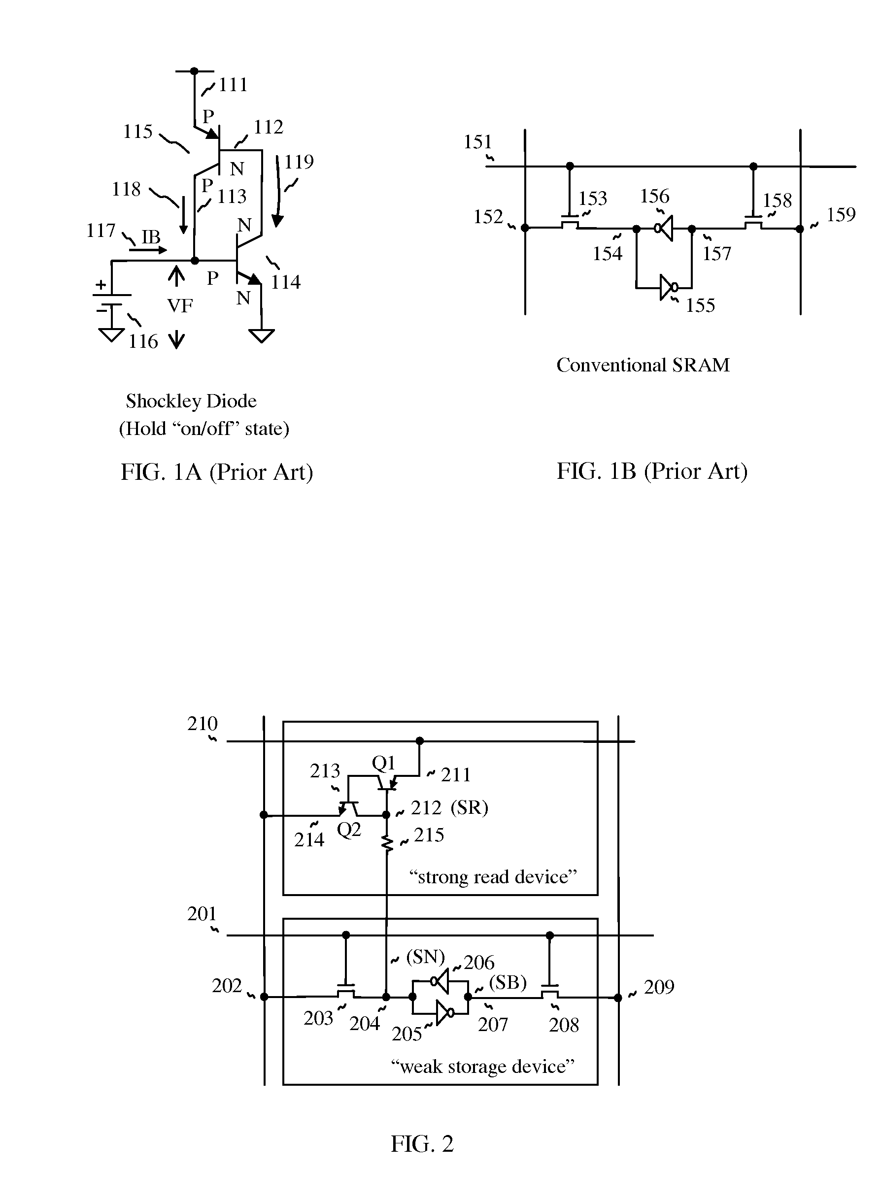
Figure 2 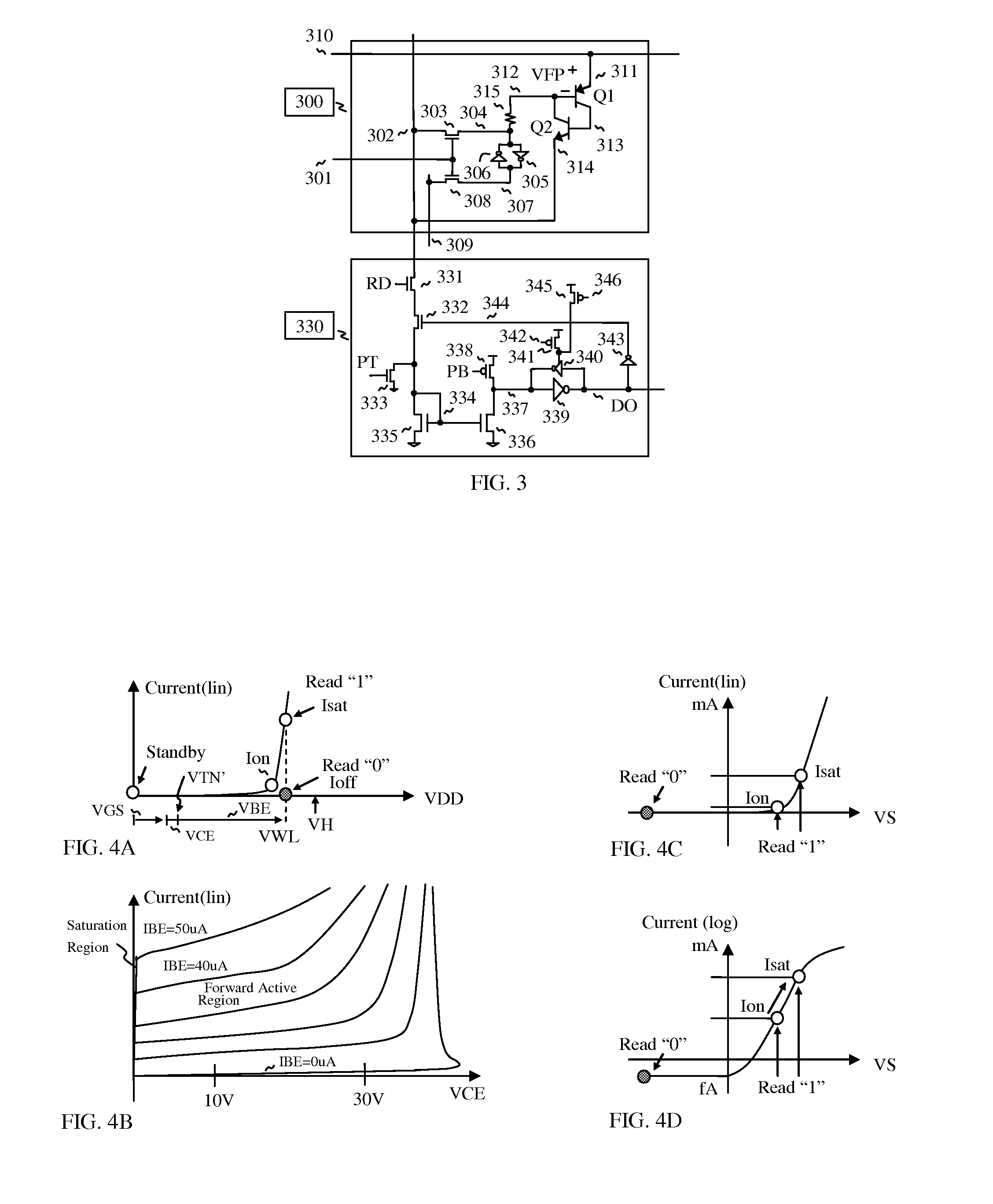
Figure 3
Abstract
Description
CROSS REFERENCE TO RELATED APPLICATION
[0001] The present invention is a continuation of application Ser. No. 11 / 755,197, filed on May 30, 2007, which is a continuation of application Ser. No. 11 / 164,919, filed on Dec. 11, 2005, now U.S. Pat. No. 7,196,926, which are herein incorporated by reference.FIELD OF THE INVENTION
[0002] The present invention relates generally to integrated circuits, in particular to SRAM (Static Random Access Memory) including a static storage element, and its applications, such as single port memory, multi port memory and CAM (content addressable memory). BACKGROUND OF THE INVENTION
[0003] A p-n-p-n diode known as Shockley diode or thyristor, is a solid-state semiconductor device similar to two-terminal p-n diode, with an extra terminal which is used to turn it on. Once turned on, diode (p-n-p-n diode or n-p-n-p diode) will remain on conducting state as long as there is a significant current flowing through it. If the current falls to zero, the device swit...
Examples
Embodiment Construction
)
[0046] Reference is made in detail to the preferred embodiments of the invention. While the invention is described in conjunction with the preferred embodiments, the invention is not intended to be limited by these preferred embodiments. On the contrary, the invention is intended to cover alternatives, modifications and equivalents, which may be included within the spirit and scope of the invention as defined by the appended claims. Furthermore, in the following detailed description of the invention, numerous specific details are set forth in order to provide a thorough understanding of the invention. However, as is obvious to one ordinarily skilled in the art, the invention may be practiced without these specific details. In other instances, well-known methods, procedures, components, and circuits have not been described in detail so that aspects of the invention will not be obscured.
[0047] The present invention is directed to a static random access memory, as shown in FIG. 2. Th...