
Piezoelectric film, piezoelectric device, liquid ejection apparatus, and method of producing piezoelectric film
a piezoelectric film and liquid ejection technology, applied in the field of piezoelectric film, piezoelectric device, liquid ejection apparatus, and method of producing piezoelectric film, can solve the problems of arcing phenomenon, inability to make films thick, and ineffective lamination and crystallization formation of horizontal stripes, so as to achieve the effect of improving driving durability, preventing effective lamination and crystallization, and improving driving durability
Patent Information
- Authority / Receiving Office
- US · United States
- Patent Type
- Applications(United States)
- Current Assignee / Owner
- Publication Date
- 2011-09-08
- Estimated Expiration
- Not applicable · inactive patent
Smart Images
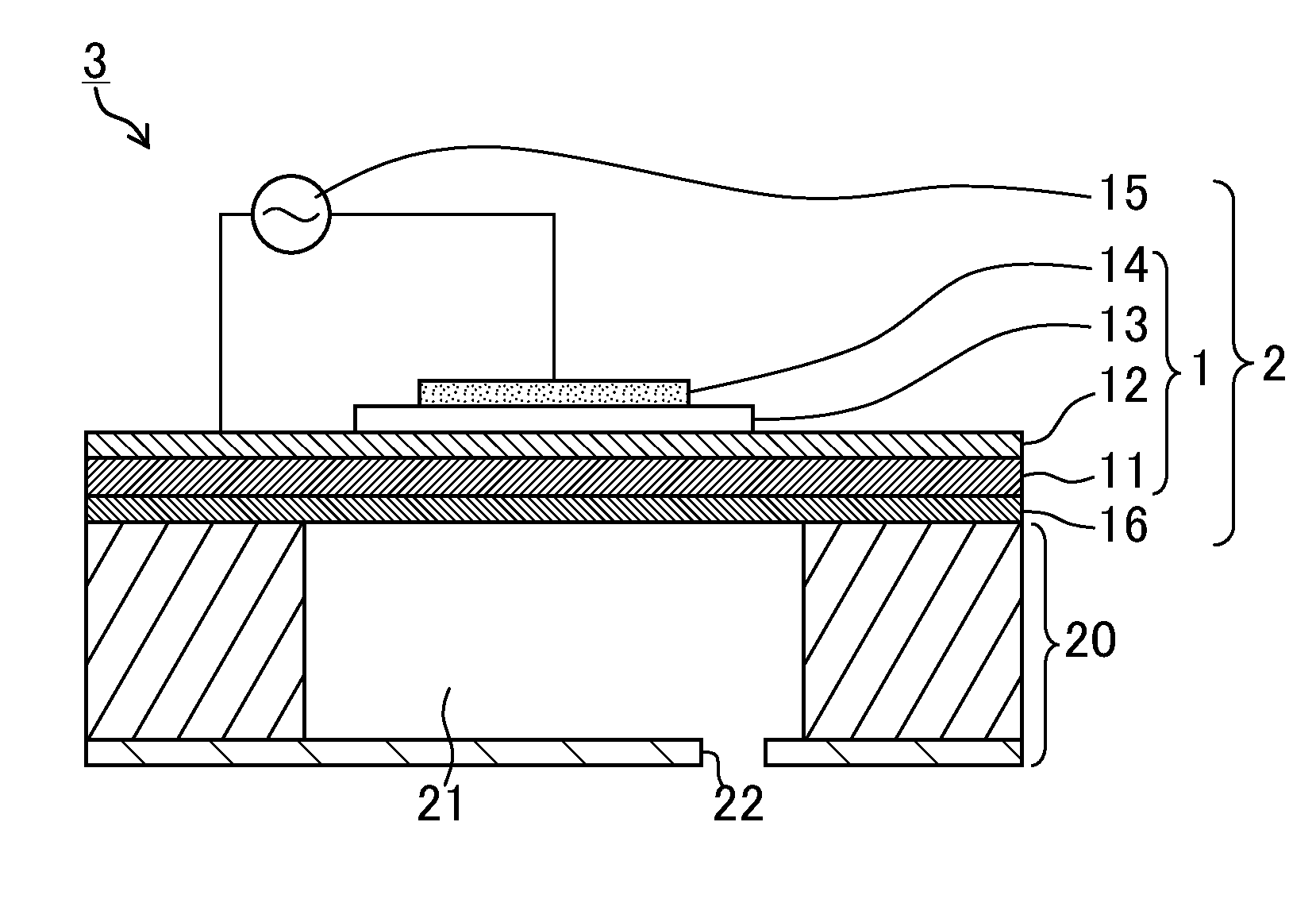
Figure 1 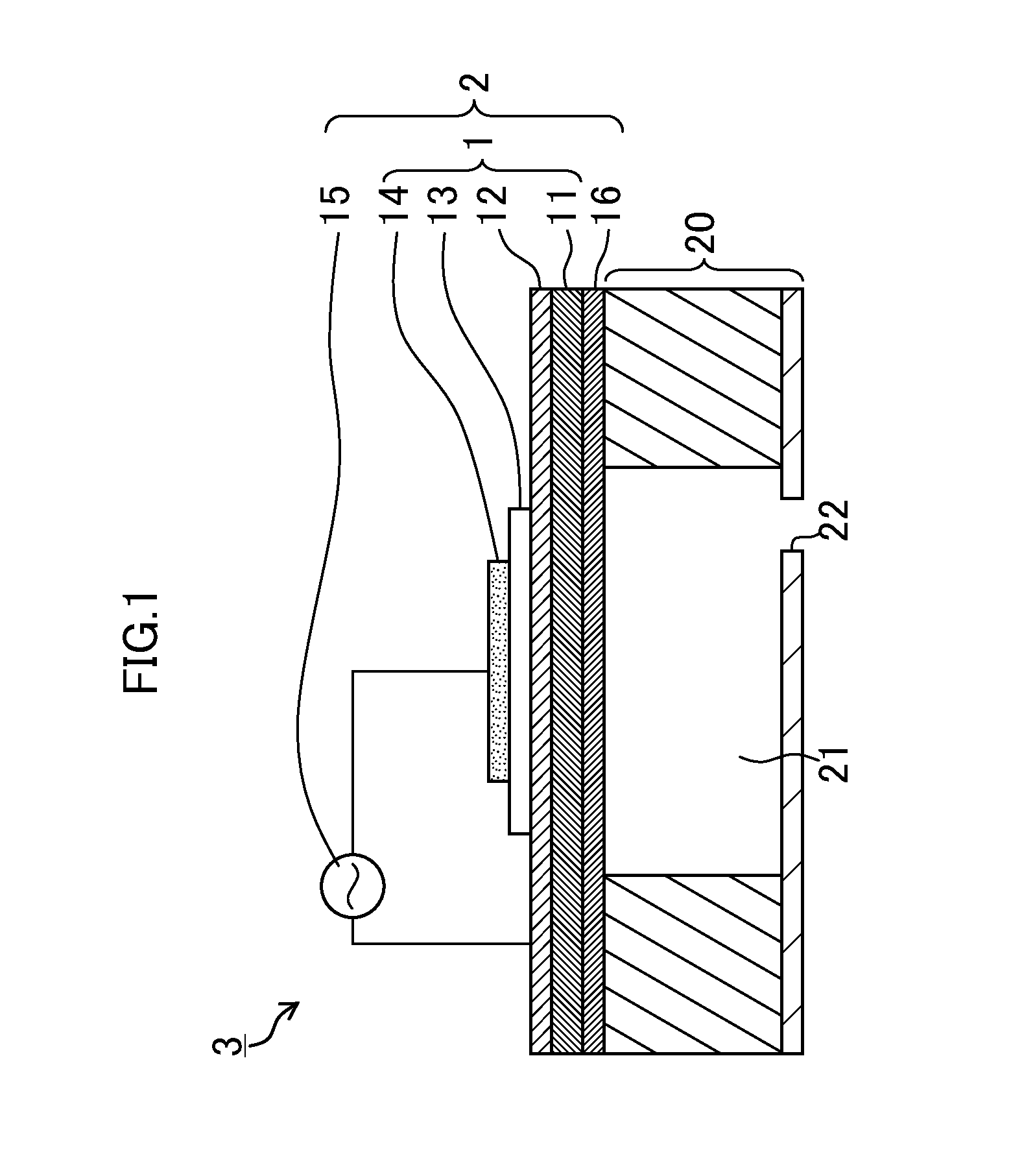
Figure 2 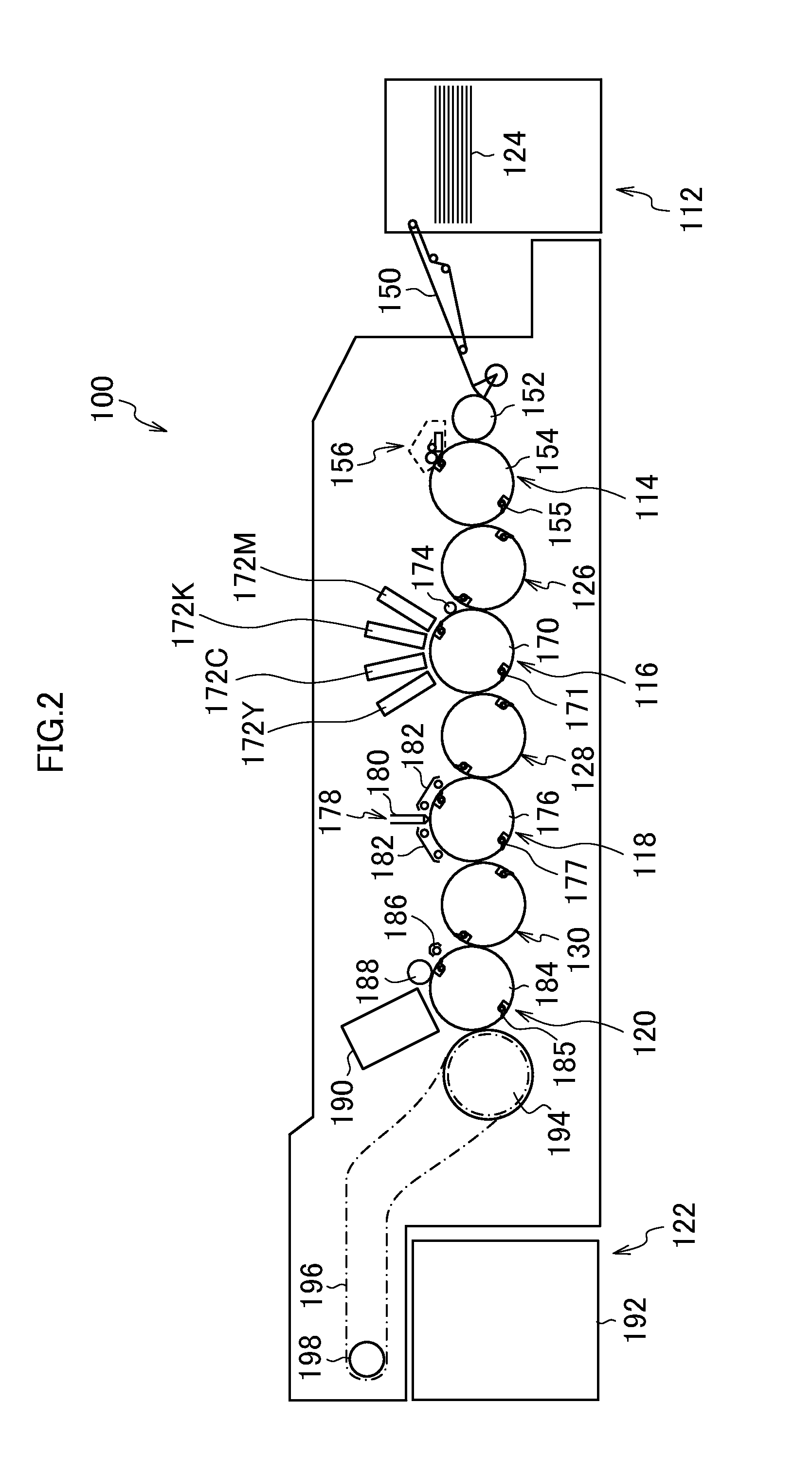
Figure 3
Abstract
Description
BACKGROUND OF THE INVENTION
[0001] 1. Field of the Invention
[0002] The present invention relates to a piezoelectric film, a piezoelectric device, a liquid ejection apparatus, and a method of producing a piezoelectric film, more particularly to a piezoelectric film with improved durability in continuous driving, a piezoelectric device including the piezoelectric film, a liquid ejection apparatus including the piezoelectric device, and a method of producing the piezoelectric film.
[0003] 2. Description of the Related Art
[0004] There has been known a piezoelectric device that is obtained by combining a piezoelectric film having a piezoelectric property displaced by application of a drive voltage, with electrodes through which the drive voltage is applied to the piezoelectric film Japanese Patent Application Publication No. 11-307833, for example, describes a piezoelectric device in which the (100) orientation in the crystal forming a piezoelectric film is inclined by 5° to 20°. Inclining the...
Examples
example 1
[0104]A Ti film with a thickness of 30 nm and an Ir film with a thickness of 150 nm were sequentially formed on an SOI substrate to obtain a lower electrode, by using the sputtering method at the substrate temperature of 350° C. A Nb-doped PZT piezoelectric film with a thickness of 4 um was formed on this lower electrode. This film formation was performed under the following conditions.
>
[0105]Film formation apparatus: RF sputtering apparatus
Target: Pb1.3((Zr0.52Ti0.48)0.88Nb0.12)O3 sintered body (the amount of Nb occupying the B-site: 12 mol %)
Substrate temperature: 475° C.
Target-substrate (T-S) distance: 60 mm
Film formation pressure: 0.30 Pa
Film formation gas: Ar / O2=97.5 / 2.5 (molar ratio)
Substrate potential Vsub=−12 V
The substrate potential Vsub was set at +25 V for five minutes after starting the film formation in order to provide a perovskite layer as an initial layer.
[0106]As a result of performing the XRD measurement to examine the orientation of the piezoelectric film after co...
examples 2 to 6
[0112]The same method as that of Example 1 was used for producing piezoelectric films and inkjet recording heads under the conditions described in FIG. 5, and the obtained piezoelectric films and inkjet recording heads were evaluated.