

Semiconductor device and method for forming the same
a technology of semiconductors and devices, applied in the direction of semiconductor devices, basic electric elements, electrical equipment, etc., can solve the problems of reducing the reliability of nmos transistors, and achieve the effects of increasing stresses, enhancing transistor performance, and increasing compressive stresses between epitaxial layers and channel regions
Patent Information
- Authority / Receiving Office
- US · United States
- Patent Type
- Applications(United States)
- Current Assignee / Owner
- Publication Date
- 2012-06-07
Smart Images
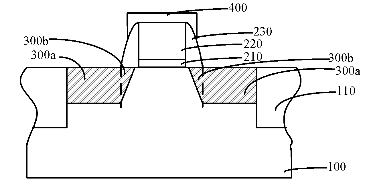
Figure 1 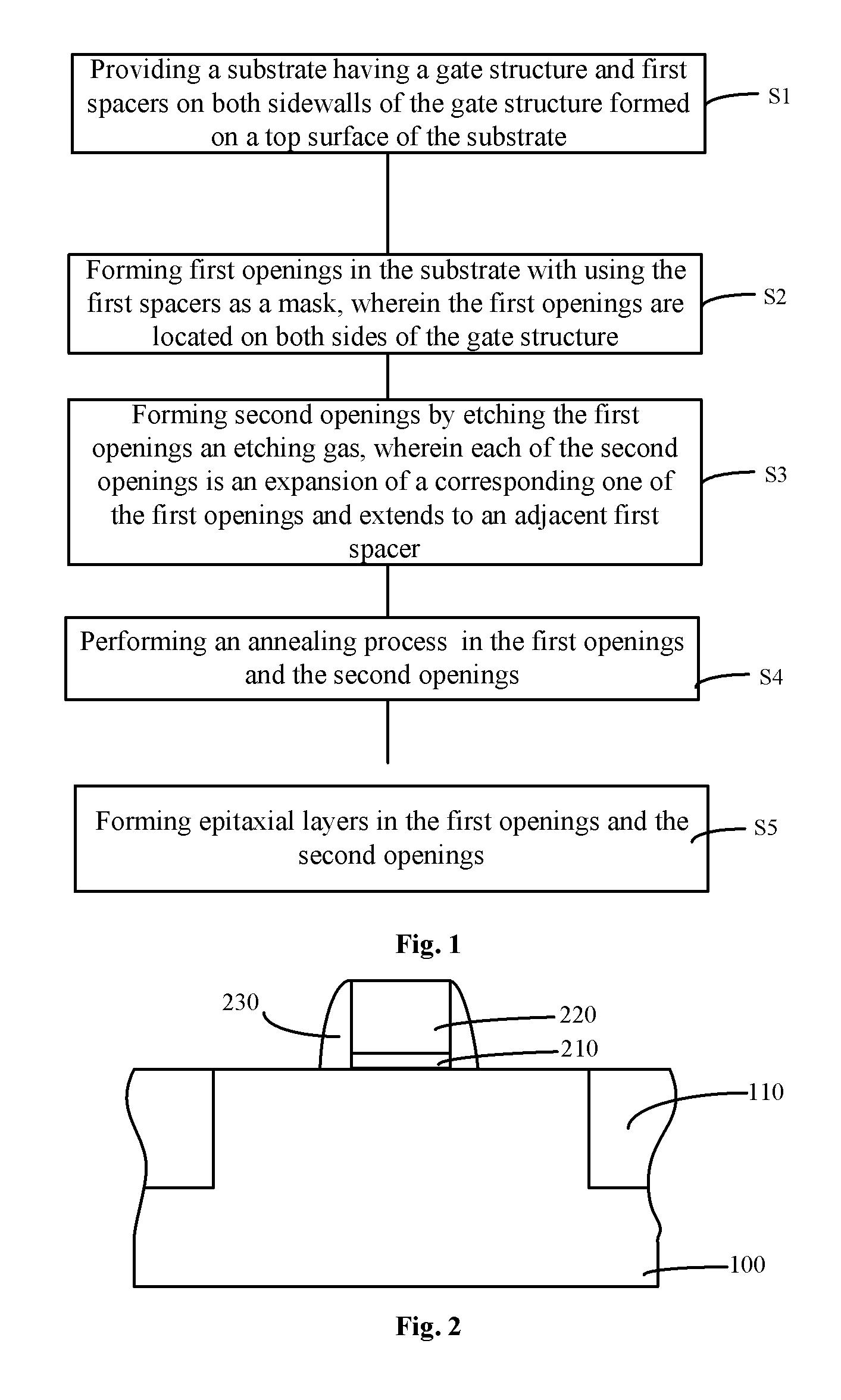
Figure 2 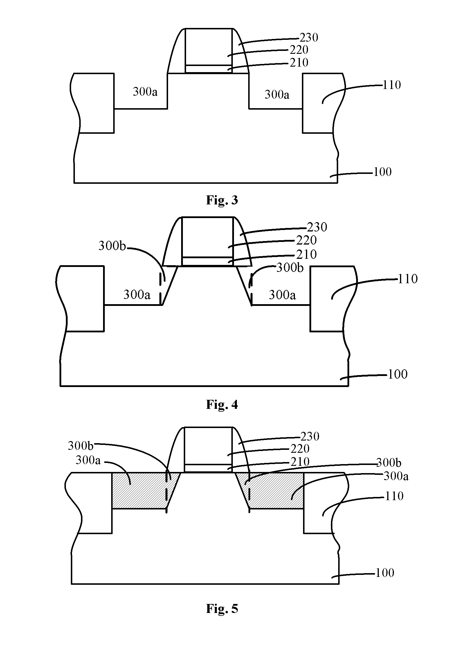
Figure 3
Abstract
Description
CROSS REFERENCE TO RELATED APPLICATIONS
[0001] The present application claims the priority of Chinese Patent Application No. 201010569390.6, entitled “Semiconductor Device and Method for Forming the Same”, and filed on Dec. 1, 2010, the entire disclosure of which is incorporated herein by reference.FIELD OF THE INVENTION
[0002] The present invention generally relates to the semiconductor manufacturing field, and more particularly, to a semiconductor device and a method for forming the semiconductor device.BACKGROUND OF THE INVENTION
[0003] It is well known that carrier mobility and energy gap of silicon can be changed by a mechanical stress. And, recently, the mechanical stress plays a more and more important role in influencing performance of MOSFETs. If the carrier (electrons in NMOS transistors or holes in PMOS transistors) mobility can be increased by appropriate control of the mechanical stress, the drive current can be increased. In other words, the performance of MOSFETs can be imp...
Examples
Embodiment Construction
[0057]In the prior art, while forming epitaxial layers on MOS transistors, distances between two adjacent epitaxial layers can be reduced by reducing widths of spacers, so that stresses between the epitaxial layers and the channel regions of the MOS transistors are increased. However, the reduction of the widths of the spacers of some MOS transistors on which no epitaxial layers are formed may impair the protective effect for the gate structures, or even cause the gate structures to be exposed in an environment for forming the epitaxial layers, which may reduce reliability of a semiconductor device.
[0058]To solve the problems mentioned above, an embodiment of the present invention provides a method for forming a semiconductor device, including: providing a substrate, wherein a gate structure and first spacers on both sidewalls of the gate structure are formed on the substrate; forming first openings in the substrate by using the first spacers as a mask, wherein the first openings ar...