
Semiconductor memory device, semiconductor system and reading method
a memory device and semiconductor technology, applied in the field of semiconductor memory devices, can solve the problems of insufficient protection, inability of the memory system to operate normally, increased risk of information leakage, etc., and achieve the effect of improving the security level of specific data
Patent Information
- Authority / Receiving Office
- US · United States
- Current Assignee / Owner
- Publication Date
- 2015-11-12
Smart Images
Figure 1 
Figure 2 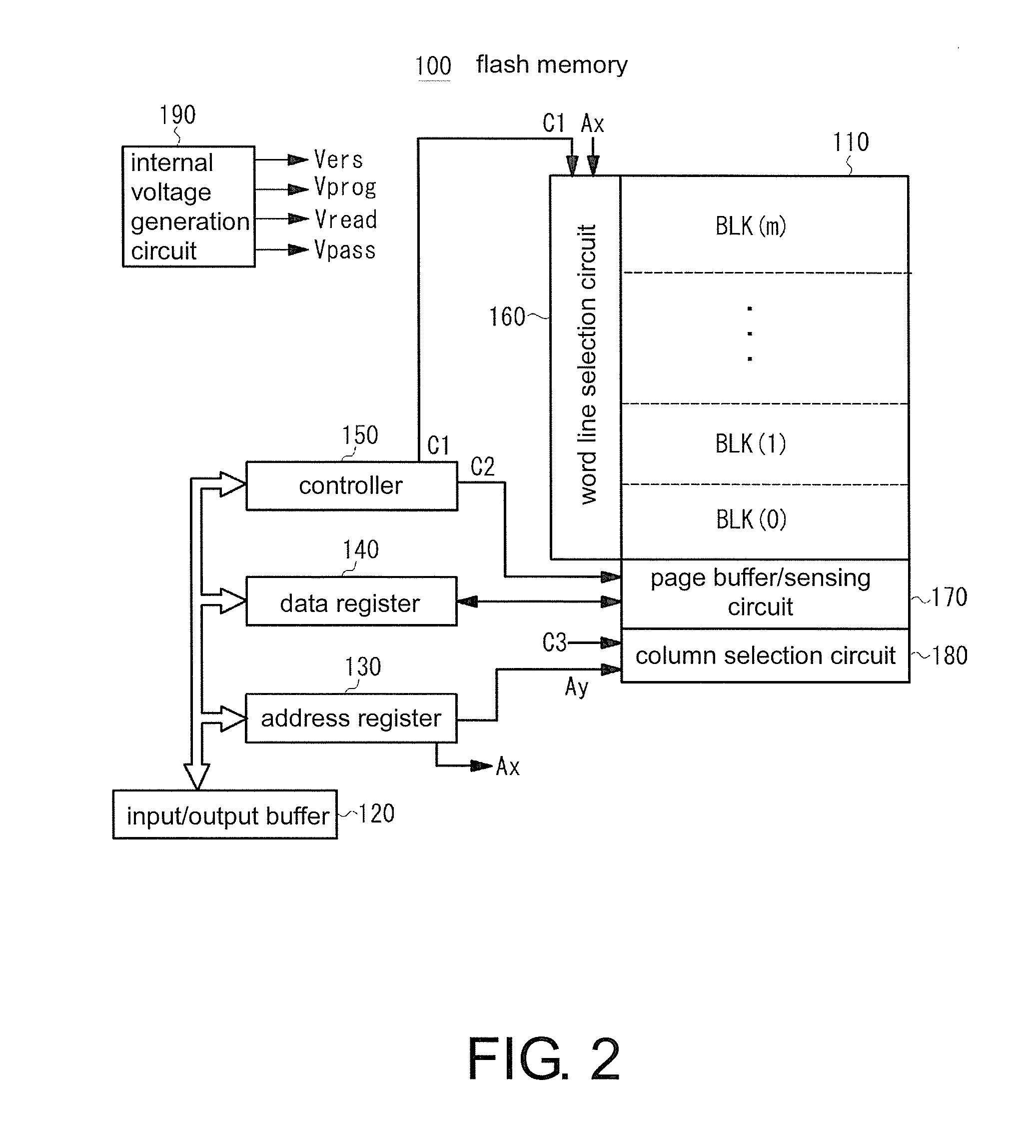
Figure 3
Abstract
Description
CROSS-REFERENCE TO RELATED APPLICATION
[0001] This application claims the priority benefit of Japan application serial no. 2014-096667, filed on May 8, 2014. The entirety of the above-mentioned patent application is hereby incorporated by reference herein and made a part of this specification.BACKGROUND OF THE INVENTION
[0002] 1. Field of the Invention
[0003] The invention relates to a semiconductor memory device such as a Not AND (NAND) flash memory, and particularly relates to storing and reading of information with a high security level.
[0004] 2. Description of Related Art
[0005] A NAND flash memory has a memory cell array, and the memory cell array includes a NAND string serially connecting a plurality of memory cells. Compared with a NOT OR (NOR) flash memory, the NAND flash memory is capable of realizing a memory cell array having a high density, and is thus suitable for data storage with a large capacity for image or music data. In addition to such purpose, the NAND flash memory also ...
Examples
Embodiment Construction
[0032]In the following, the embodiments of the invention are described in detail with reference to the accompanying drawings. FIG. 2 is a diagram illustrating a configuration of a flash memory according to an embodiment of the invention. However, the configuration of the flash memory illustrated herein only serves as an illustrative example. The invention is not limited to the configuration illustrated herein.
[0033]As shown in FIG. 2, a flash memory 100 of this embodiment is configured to include a memory array 110 formed with a plurality of memory cells arranged in an array, an input / output buffer 120 connected to an external input output terminal I / O and keeping input and output data, an address register 130 receiving an address data from the input / output buffer 120, a data register 140 keeping the input and output data, and a controller 150 providing control signals C1, C2, C3, etc., to the respective parts based on command data from the input / output buffer 120 and an external co...