
Display device and electronic device
a display device and electronic technology, applied in the field of display devices, can solve the problems of imposing limitations on the shape of the display region and significant limitations in the housing design, and achieve the effects of reducing frame width, minimizing the external shape of the display device, and high degree of flexibility of the display region
Patent Information
- Authority / Receiving Office
- US · United States
- Patent Type
- Applications(United States)
- Current Assignee / Owner
- Publication Date
- 2015-12-24
- Estimated Expiration
- Not applicable · inactive patent
Smart Images
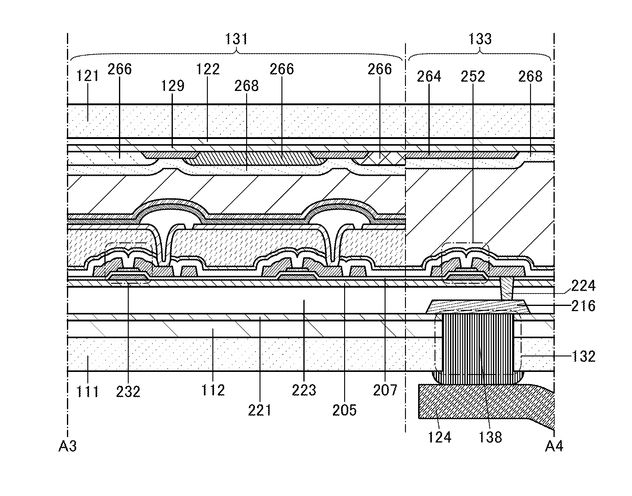
Figure 1 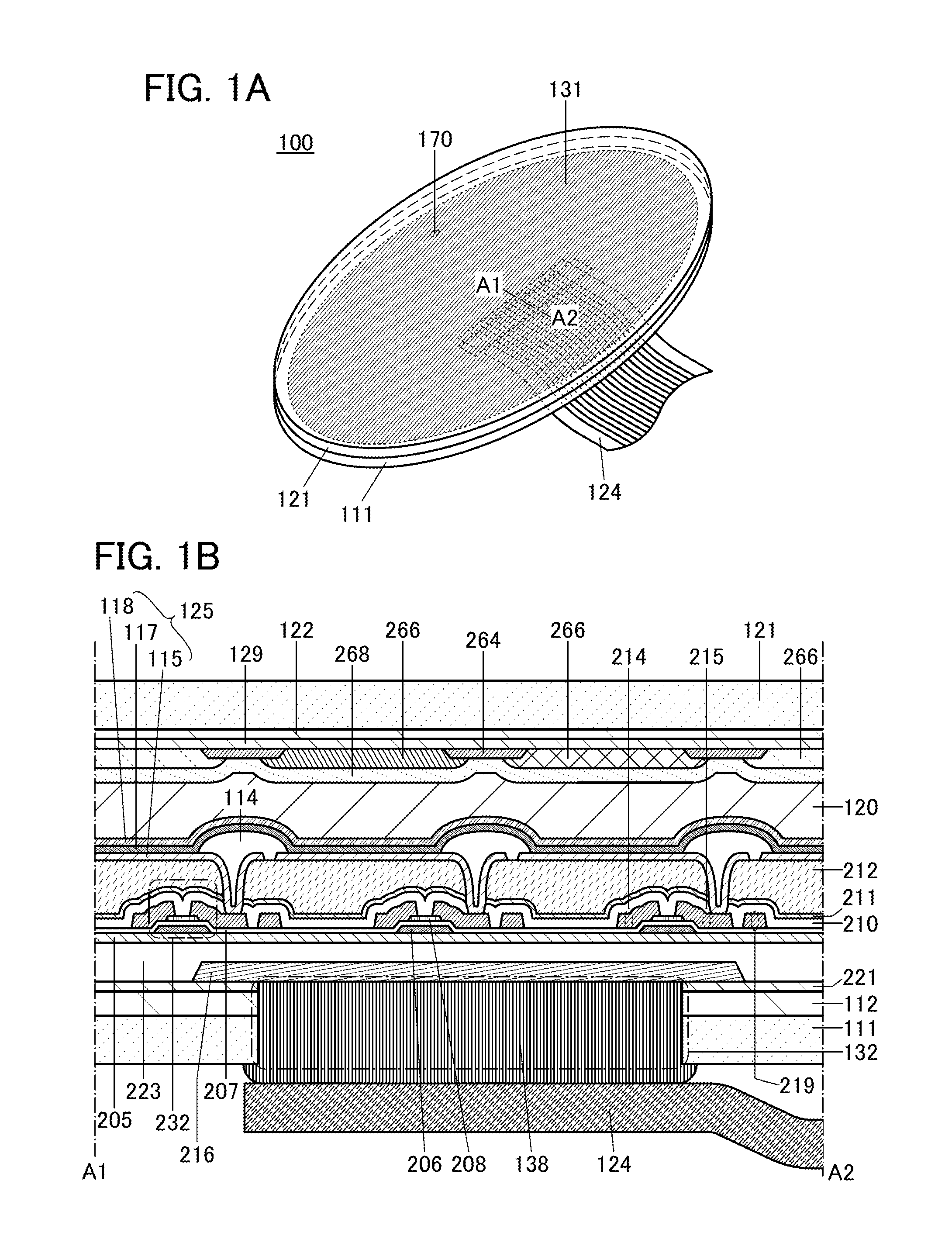
Figure 2 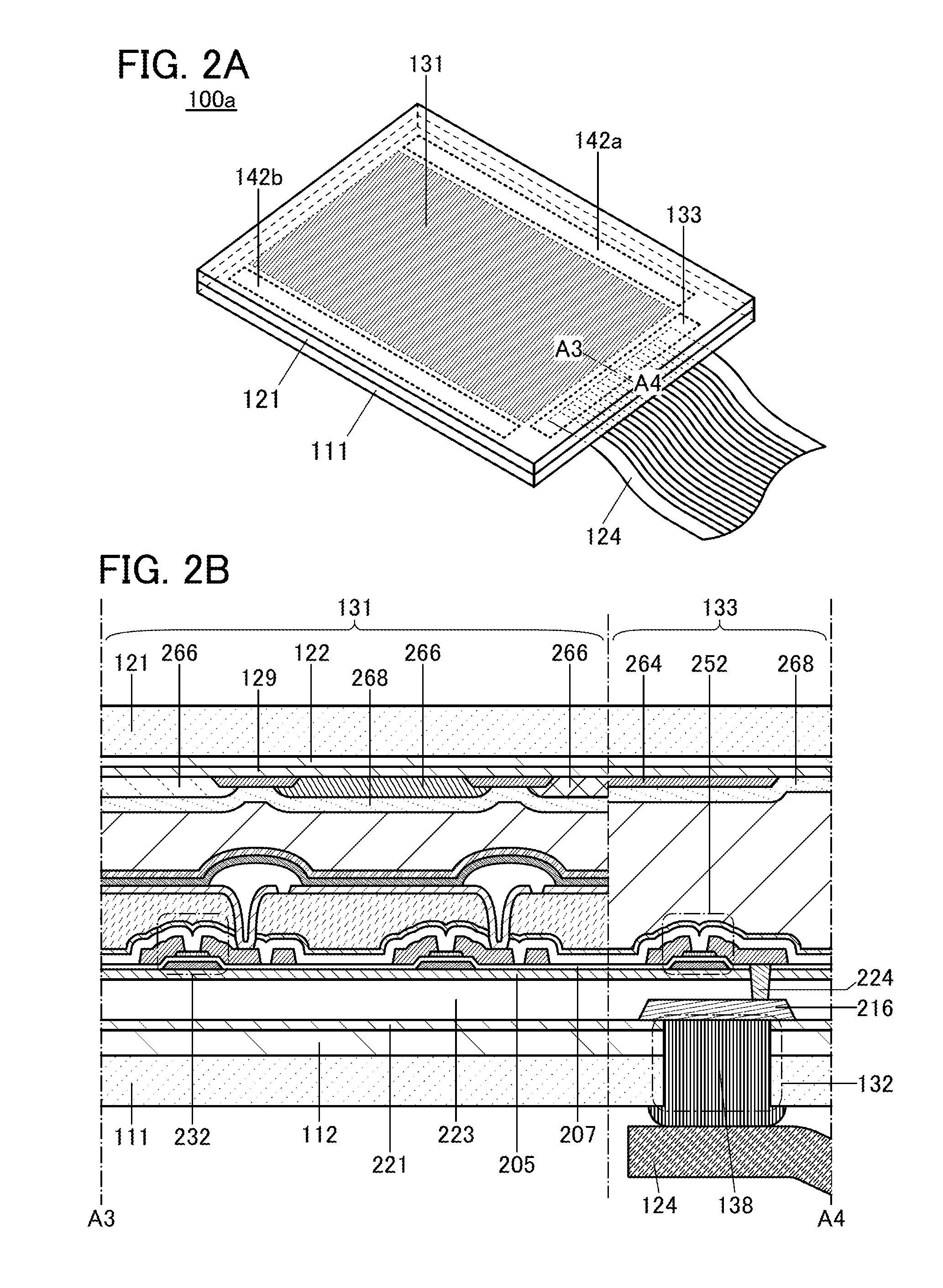
Figure 3
Abstract
Description
TECHNICAL FIELD
[0001] The present invention relates to a display device. The present invention also relates to a method of manufacturing the display device.
[0002] One embodiment of the present invention is not limited to the above technical field.
[0003] The technical field of one embodiment of the invention disclosed in this specification and the like relates to an object, a method, or a manufacturing method. In addition, one embodiment of the present invention relates to a process, a machine, manufacture, or a composition of matter.
[0004] The term display device refers to a device including a display element. The display device may include a driver circuit driving a plurality of pixels, a control circuit, a power supply circuit, a signal generation circuit, or the like. The term display device may refer to, for example, a module to which a connector such as a flexible printed circuit (FPC), tape automated bonding (TAB) tape, or a tape carrier package (TCP) is attached, a module in whic...
Examples
embodiment 1
[0084]Examples of a structure of a display device 100 and a manufacturing method thereof according to one embodiment of the present invention are described with reference to drawings.
example 1
[Structure Example 1 of Display Device]
[0085]FIG. 1A is a perspective view of the display device 100 to which an external electrode 124 is connected. The external shape of the display device 100 illustrated in FIG. 1A is a non-rectangular shape. The display device 100 includes a display region 131 that has a non-rectangular shape. FIG. 1B is a cross-sectional view taken along the dash-dot line A1-A2 in FIG. 1A. The display device 100 disclosed in this specification is a display device in which a light-emitting element is used as a display element. As the display device 100 of one embodiment of the present invention, a display device having a top-emission structure is described as an example.
[0086]The display device 100 described in this embodiment includes the display region 131. The display device 100 also includes a terminal electrode 216 and a light-emitting element 125 including an electrode 115, an EL layer 117, and an electrode 118. A plurality of light-emitting elements 125 a...
example 2
[Structure Example 2 of Display Device]
[0098]FIG. 2A illustrates the display device 100a having a rectangular external shape. FIG. 2A is a perspective view of the display device 100a having a rectangular shape to which the external electrode 124 is connected. FIG. 2B is a cross-sectional view taken along the dash-dot line A3-A4 in FIG. 2A. Note that components identical with those of the display device 100 illustrated in FIG. 1A are not described here.
[0099]The display device 100a illustrated in FIG. 2A includes the display region 131 having a rectangular shape. Outside the display region 131, a driver circuit 133, a driver circuit 142a, and a driver circuit 142b are provided. Note that in this specification and the like, one or more of the driver circuits 133, 142a, and 142b may be simply referred to as a driver circuit or a peripheral driver circuit.
[0100]The driver circuits 133, 142a, and 142b each include a plurality of transistors 252. The driver circuits 133, 142a, and 142b ea...