
Nano-Structured Porous Thermoelectric Generators
a porous, nano-structure technology, applied in the manufacture/treatment of thermoelectric devices, non-metal conductors, conductors, etc., can solve the problems of high material cost, high production cost, and use of rare elements, and achieve safe and economical methods for nano-sizing silicon, high seebeck coefficient, and high work capability
Patent Information
- Authority / Receiving Office
- US · United States
- Patent Type
- Applications(United States)
- Current Assignee / Owner
- Publication Date
- 2016-03-10
- Estimated Expiration
- Not applicable · inactive patent
Smart Images
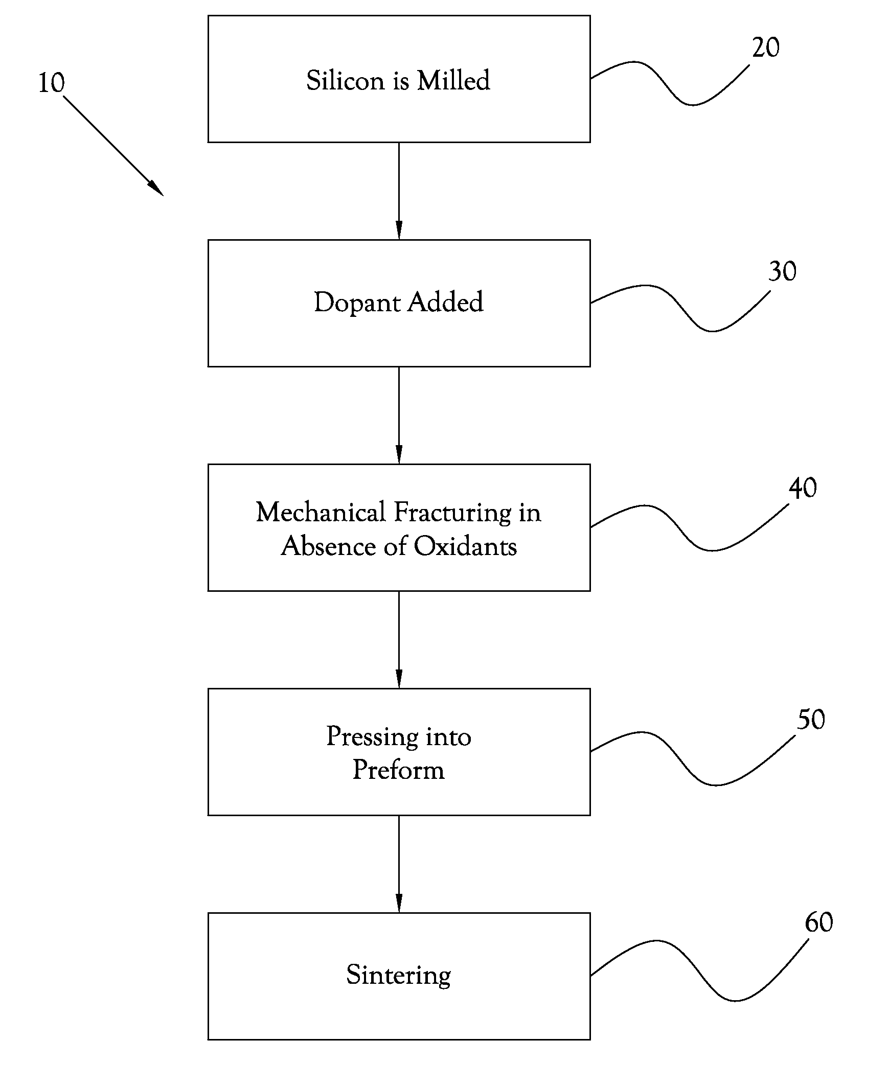
Figure 1 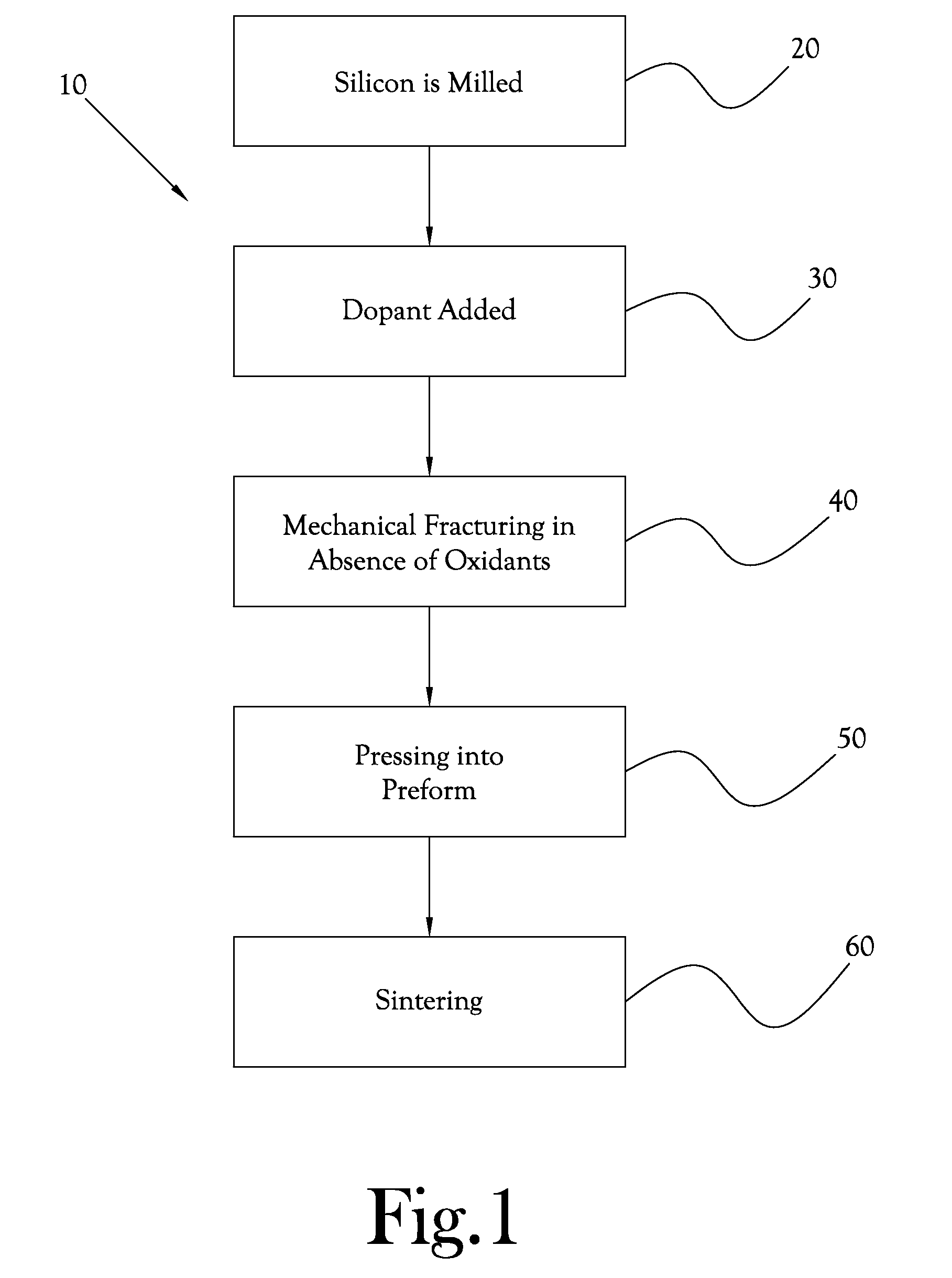
Figure 2 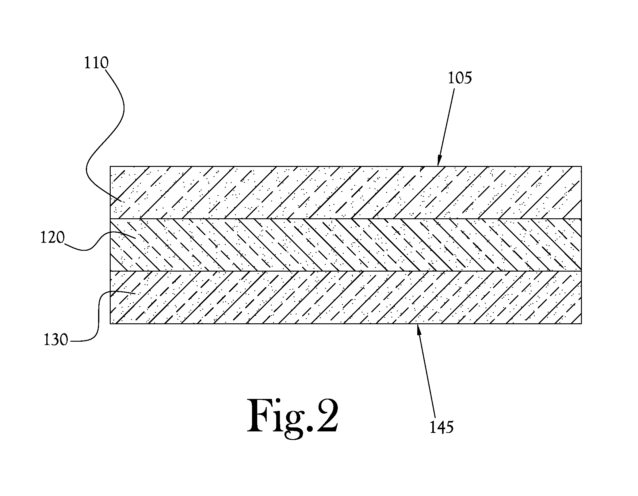
Figure 3
Abstract
Description
CROSS-REFERENCE TO RELATED APPLICATIONS
[0001] This application claims the benefit of U.S. Provisional Patent Application No. 62 / 046,434, filed Sep. 5, 2014, the content of which is incorporated by reference herein in its entirety.STATEMENT REGARDING FEDERALLY SPONSORED RESEARCH OR DEVELOPMENT
[0002] Not ApplicableBACKGROUND OF THE INVENTION
[0003] 1. Field of Invention
[0004] The present general inventive concept relates to the preparation and use of thermoelectric materials and more particularly to methods and processes to fabricate doped thermoelectric generators, especially doped silicon-based thermoelectric generators.
[0005] 2. Description of the Related Art
[0006] Semiconductive materials that exhibit the Seebeck and Peltier effects in the presence of a temperature gradient are useful for the production of electricity from waste heat. Semiconductive materials which move heat from one side to the other when presented with an electrical charge from one side to the other are useful for cool...
Examples
Embodiment Construction
[0053]Disclosed herein are methods and processes to fabricate thermoelectric materials and more particularly to methods and processes to fabricate doped silicon-based semiconductive materials to use as thermoelectrics in the production of electricity from recovered waste heat. In some example embodiments, the present invention comprises a thermoelectric material that incorporates a silicon-based semiconductor material.
[0054]Also disclosed herein are methods and processes that encompass the use a high-purity, properly-doped, nanostructured, porous silicon milled to a particle size less than a few microns, and sinter into a thick structure that will achieve a very high efficiency converting heat to electricity.
[0055]In various example embodiments of the present general inventive concept, fabrication of effective silicon-based thermoelectric devices involves: doping for high electrical conductivity for both P and N type by doping from column III and column V of the periodic chart respe...