
Optical coupling arrangement having low coupling loss and high production yield
a coupling arrangement and low coupling loss technology, applied in the field of optical coupling arrangements, can solve the problems of reducing the insertion loss of these devices, increasing the fraction of devices fabricated which must be discarded due to defects, and reducing the size of these structural features, so as to reduce the effective width of the gap, reduce the effective width, and reduce the effect of tapering
Patent Information
- Authority / Receiving Office
- US · United States
- Patent Type
- Patents(United States)
- Current Assignee / Owner
- Publication Date
- 2005-05-10
- Estimated Expiration
- Not applicable · inactive patent
Smart Images
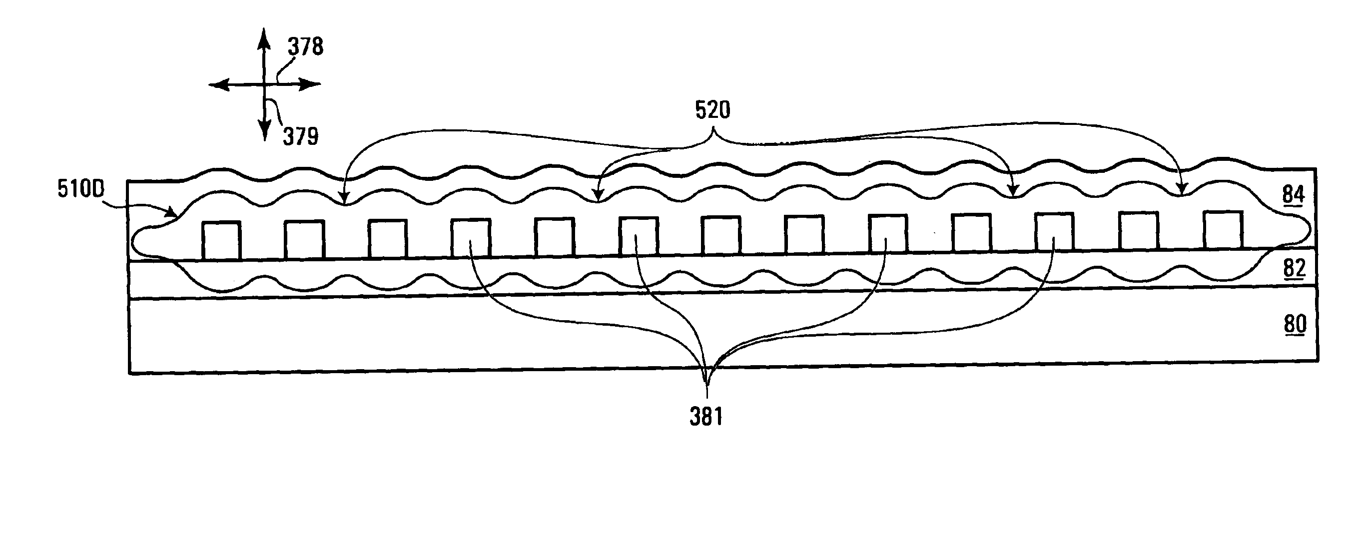
Figure 1 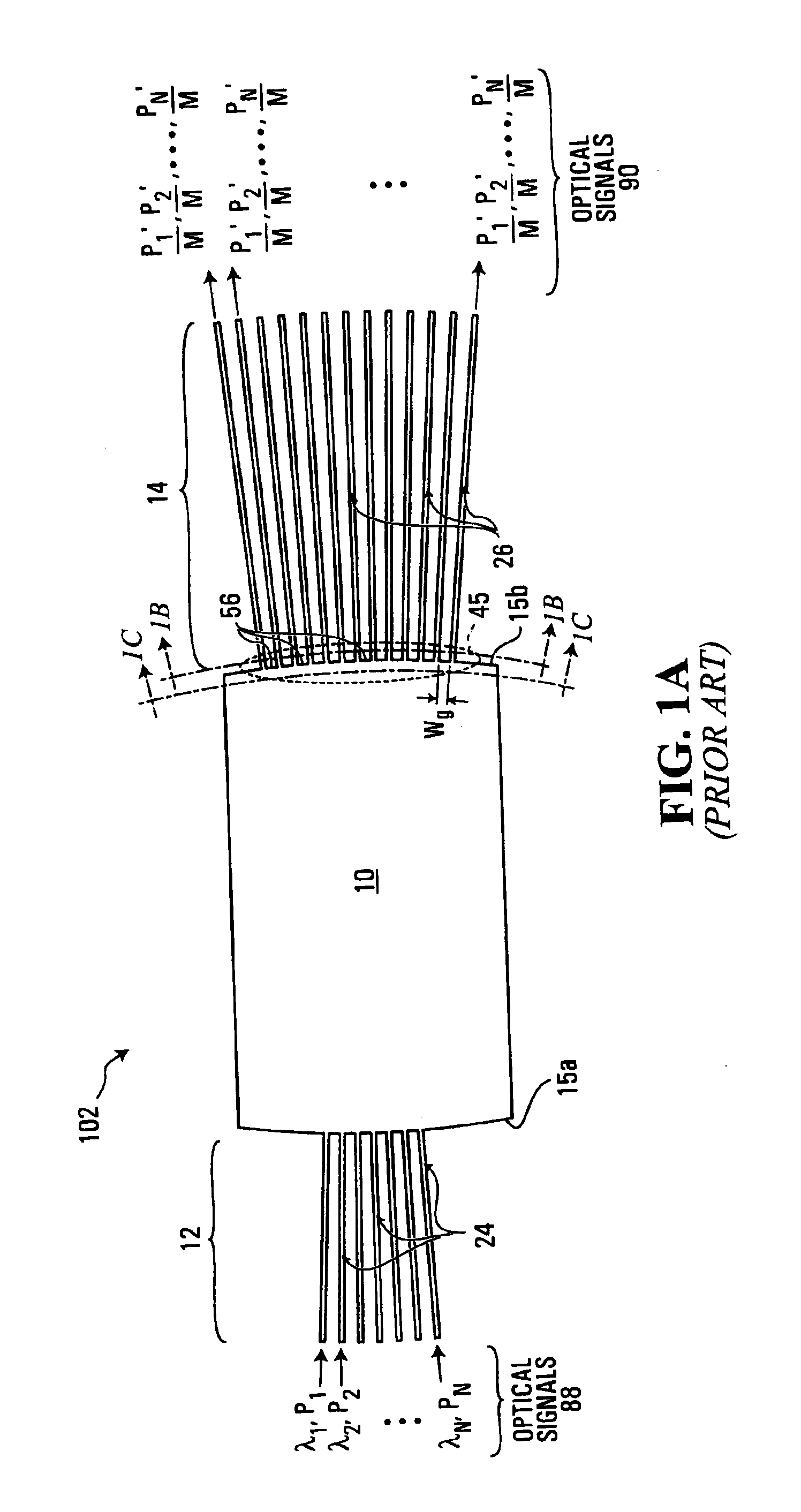
Figure 2 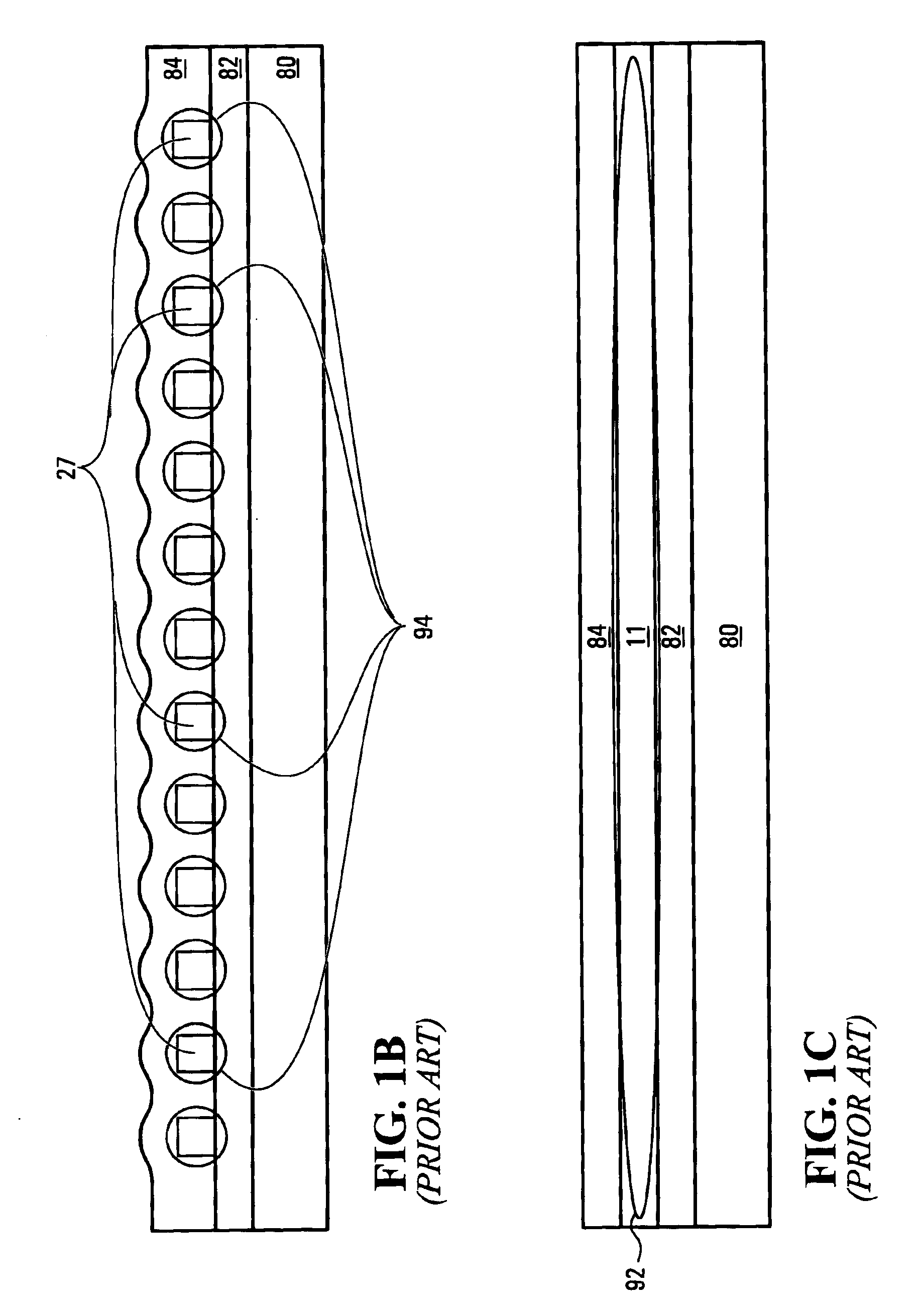
Figure 3
Abstract
Description
FIELD OF THE INVENTION
[0001] This invention relates to optical coupling arrangements for optical couplers and other optical devices using these optical couplers. In particular, the invention relates to improving the insertion loss of the optical couplers while maintaining a high production yield during manufacturing.BACKGROUND OF THE INVENTION
[0002] DWDM (Densed Wavelength Division Multiplexing) systems need optical waveguide devices such as star couplers, branch power splitters, AWG (Arrayed Waveguide Grating) multiplexers / demultiplexers and VOA (Variable Optical Attenuators) to control, combine and separate optical signals having different wavelengths. These optical waveguide devices typically have a planar waveguide structure and the insertion loss of these devices decreases with decreasing size of some of the structural features of the structure. However, during production the fraction of devices fabricated which must be discarded due to defects increases with decreasing size of t...
Examples
Embodiment Construction
[0038]Referring to FIG. 3A shown is a top view of an example star coupler according to one embodiment of the invention. The star coupler is generally indicated by 301 and has a first coupling waveguide, shown as slab waveguide 310, with preferably circularly curved ends 315a and 315b. In FIG. 3C, a cross-sectional view of the optical coupler 301 through the slab waveguide 310 shows a core 311 of the slab waveguide 310 located between layers 82 and 84 of under-cladding and top-cladding, respectively. Referring back to FIG. 3A, there is a first array 314 of first waveguides 326 and a second array 312 of second waveguides 324 at curved end 315a. A first transition region 332 has first and second ends 357 and 358, respectively, and is adjacent the slab waveguide 310. A second transition region 322 is located between the first transition region 332 and the first array 314.
[0039]The first transition region 332 has a plurality of first transverse segments 360 of a core material, and a plur...