
Memory device with a selection element and a control line in a substantially similar layer
a memory device and control line technology, applied in semiconductor devices, diodes, electrical devices, etc., can solve the problems of sensitivity to alignment tolerances, more complex devices require more individual layers to implement, and generally do not retain information stored or programmed within, so as to reduce the complexity of vertical stacking, and mitigate the effect of vertical stacking
Patent Information
- Authority / Receiving Office
- US · United States
- Patent Type
- Patents(United States)
- Current Assignee / Owner
- Publication Date
- 2008-06-24
Smart Images
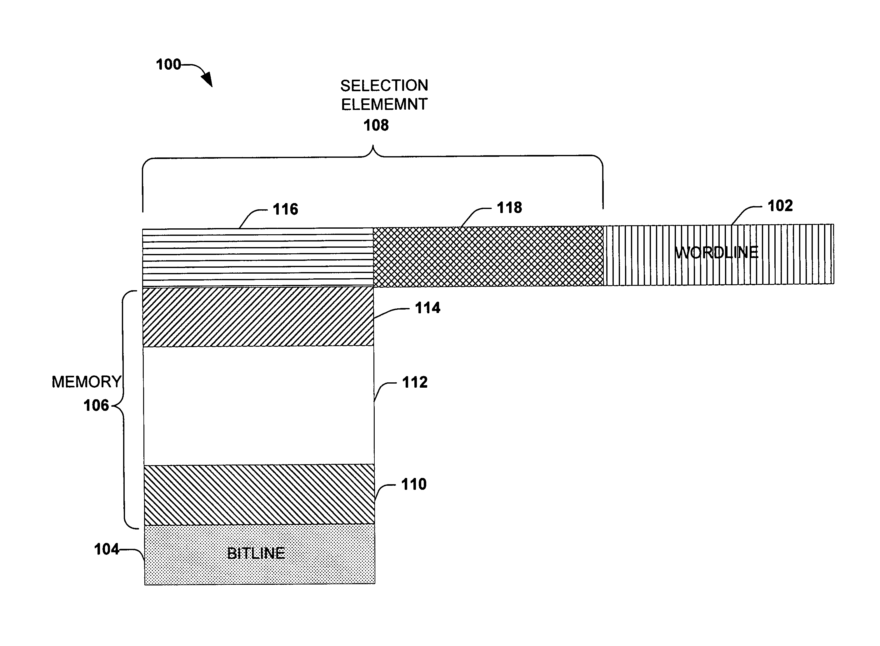
Figure 1 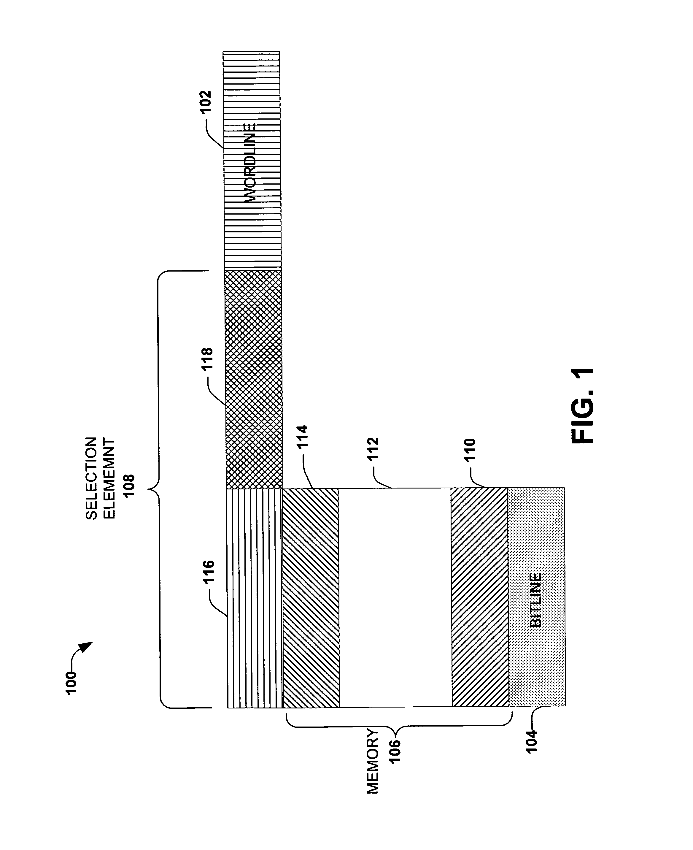
Figure 2 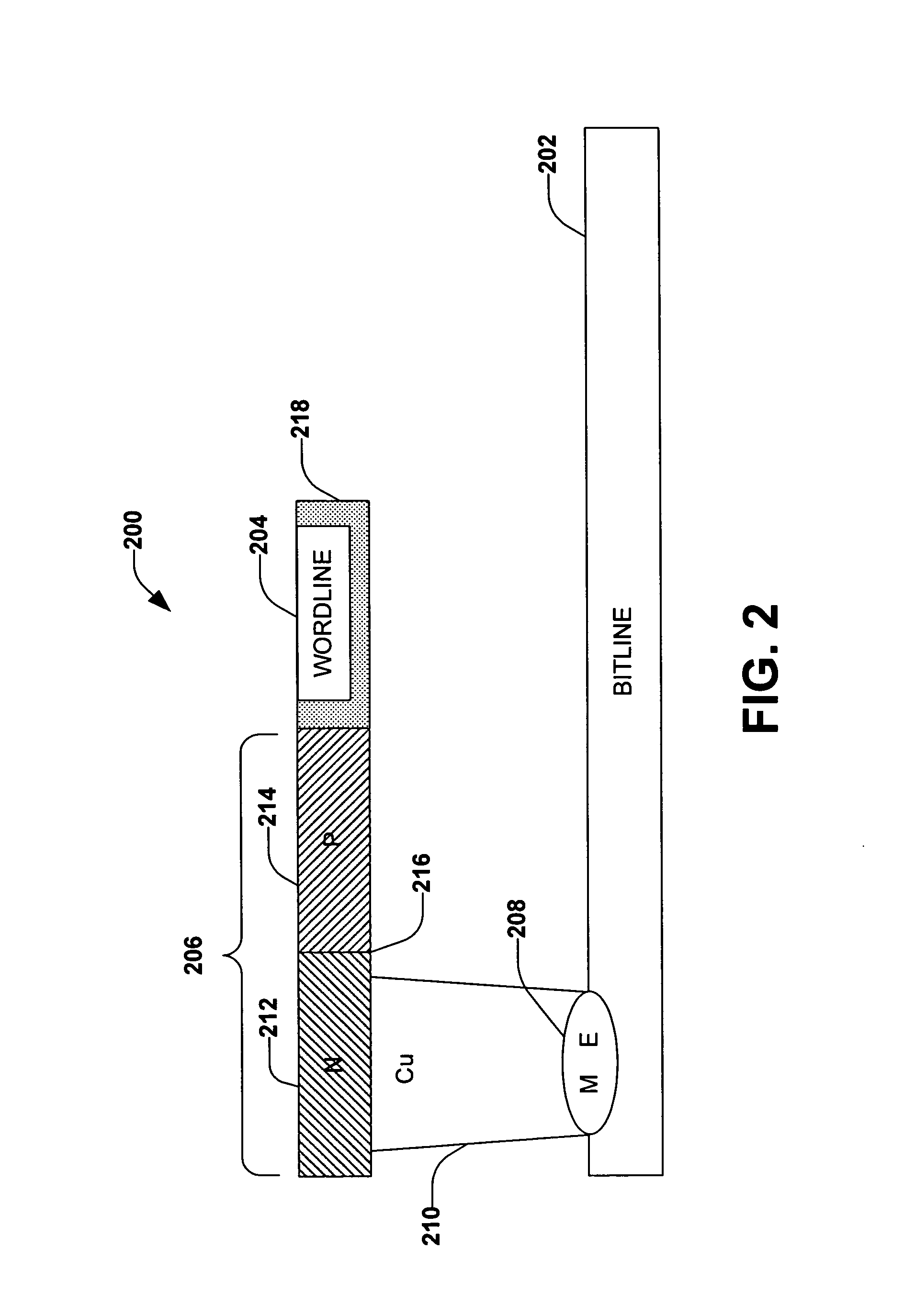
Figure 3
Abstract
Description
FIELD OF INVENTION
[0001] The subject invention relates generally to semiconductor devices and, in particular, to a semiconductor memory device with a selection element and a control line in a substantially similar layer of the semiconductor memory device.BACKGROUND OF THE INVENTION
[0002] The reduction in size of semiconductor components and increased usage of semiconductor processors has lead to an explosion of new electronic devices. Most, if not all, of these electronic devices require some amount of memory in order to function. The proliferation of such devices has significantly increased demand for memory that is efficient in size as well as power consumption. Smaller sized semiconductor components and memories have made numerous hand held electronic devices feasible. Examples of hand-held devices include cell phones, personal radios, walkie-talkies, personal data assistants, palm pilots, pagers, notebook computers, remote controls, voice recorders, audio recorders, video recorder...
Examples
Embodiment Construction
[0025]The subject invention provides a semiconductor memory device with a selection element in a substantially similar layer as a control line, which can reduce complexity associated with vertical stacking techniques utilized to implement memory devices. The invention further provides methods of making such memory devices. The selection element facilitates selection of a specific memory element to be written, read, or erased. Traditional memory devices generally form the selection element through the deposition of separate layers within a semiconductor chip, and many conventional memory arrays stack memory devices, for example, one upon another, in a vertical manner, which can increase the number of memory devices stacked upon another. The subject invention reduces complexity of vertical stacking by incorporating the selection element (e.g. a diode) into the layer where one of the control lines (e.g. a wordline and a bitline) resides. In one aspect of the invention, the selection el...