
Dielectric-filled transmission lines
a technology of dielectric filling and transmission lines, applied in the field of electric conductors, can solve the problems of increasing complexity and density of circuit boards, affecting the development of circuit boards, and affecting the electrical properties of lines, so as to reduce dielectric loss, and reduce the loss of dielectrics.
Patent Information
- Authority / Receiving Office
- US · United States
- Patent Type
- Patents(United States)
- Current Assignee / Owner
- Publication Date
- 2008-10-07
- Estimated Expiration
- Not applicable · inactive patent
Smart Images
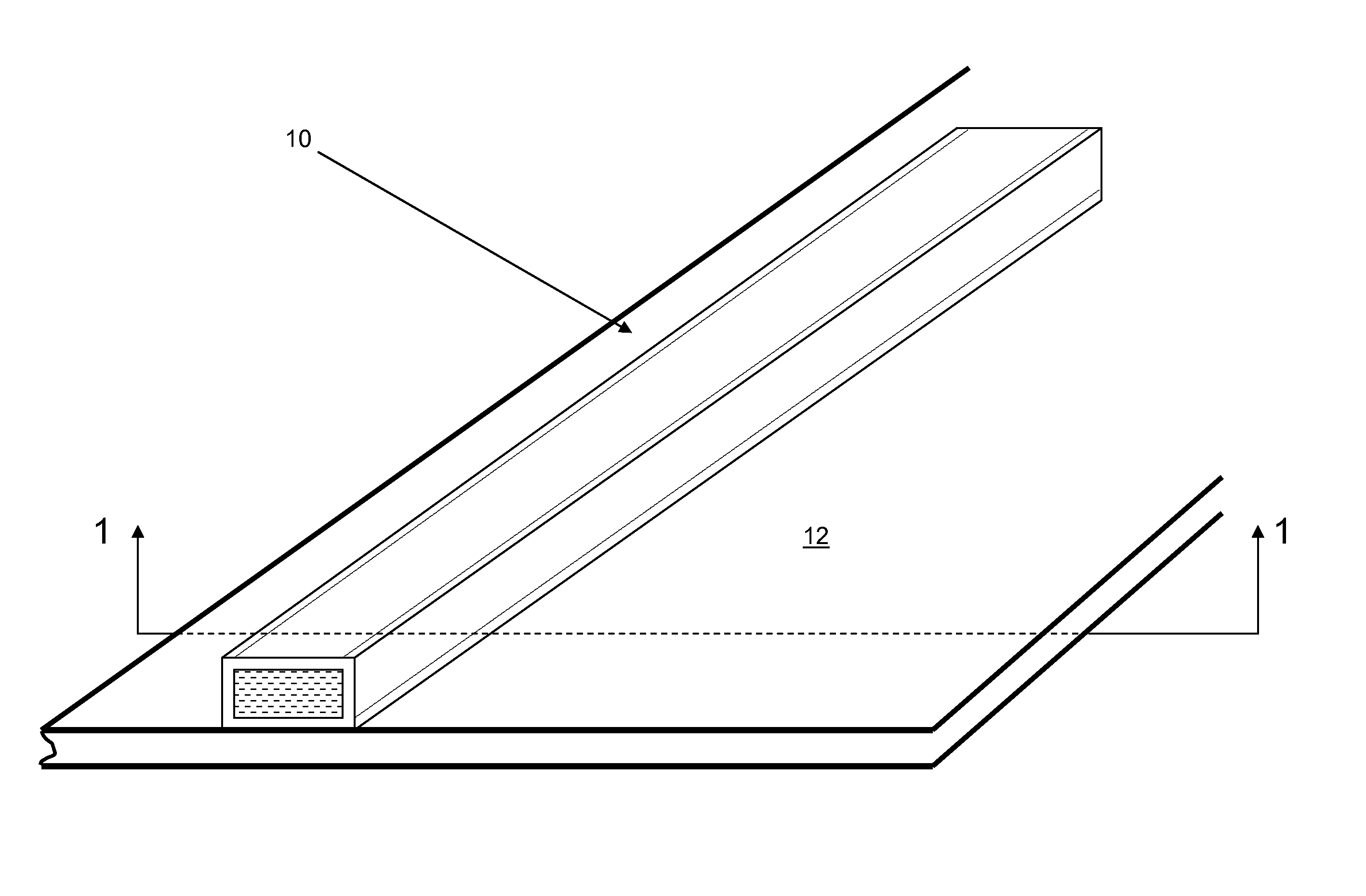
Figure 1 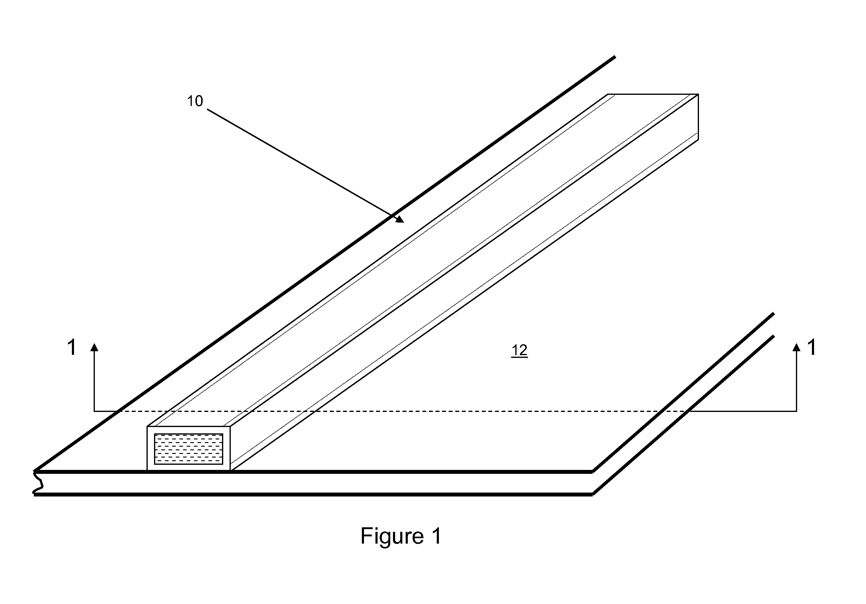
Figure 2 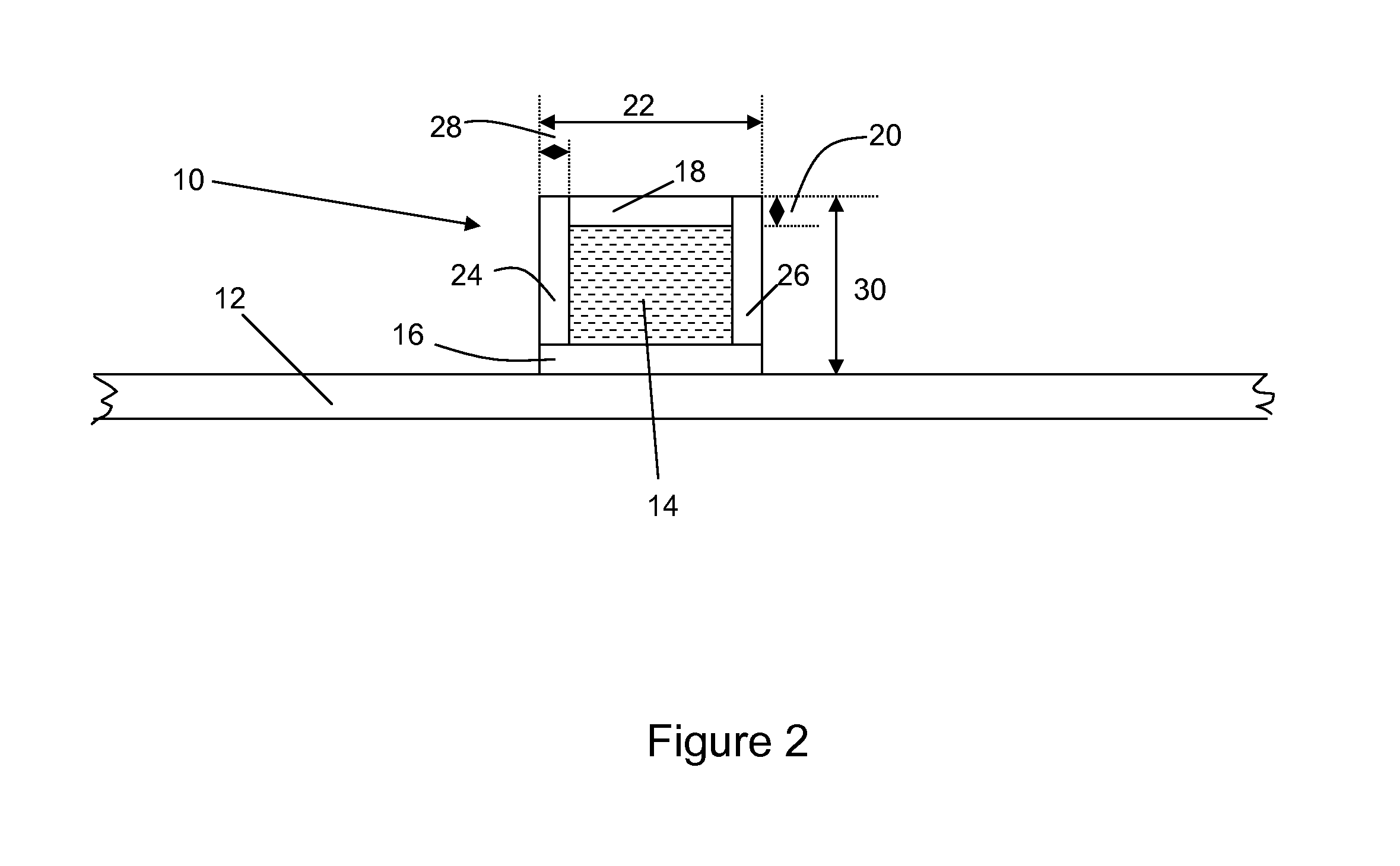
Figure 3
Abstract
Description
FIELD OF THE INVENTION
[0001] This invention is generally related to electrical conductors, and more particularly to electrical conductors on printed circuit boards.BACKGROUND OF THE INVENTION
[0002] It is generally desirable to provide electronic products in the smallest practical size. Consequently, there is a long term development trend of reducing the size of various electronic components such as integrated circuits, passive components, power supplies, and printed circuit boards. In the case of printed circuit boards, this trend has prompted development of circuit boards with ever-increasing complexity and density. Increases in density are typically associated with reduction of both the width of transmission lines and the separation between transmission lines to the extent practical with existing manufacturing technology. Current manufacturing techniques enable reliable production of printed circuit board with very small transmission lines. While this is beneficial to increasing the...
Examples
Embodiment Construction
[0022]Referring to FIGS. 1 and 2, a printed circuit board transmission line 10 disposed on a substrate 12 has a tube-like outer conductive wall surrounding an inner dielectric core 14 (see FIG. 4). As seen in FIG. 2, the outer conductive wall includes four conductive sidewalls 16, 18, 24, 26 which are connected to form a continuous, uninterrupted structure having a rectangular cross-section. It should be noted however that other cross-sectional geometries including but not limited to triangular, circular, and any four-sided structure may be employed. First and second ones of the sidewalls 16, 18 are formed from copper or other electrically conductive material in a manner known for formation of conductive traces on a substrate layer of a printed circuit board. Further, the first and second sidewalls may have a thickness 20 similar to known conductive traces, such as 10-25 microns. The conductive wall has a width 22 similar to known conductive traces, such as 50-400 microns. Third and...