
Electro-optical device, driving circuit of electro-optical device, and electronic apparatus
a technology of electrooptical devices and driving circuits, applied in instruments, pisciculture and aquaria, computing, etc., can solve problems such as ghosting along gray-scale levels, predetermined voltages cannot be applied to each of the data lines, and delay of gray-scale signals with respect to sampling periods
Patent Information
- Authority / Receiving Office
- US · United States
- Patent Type
- Patents(United States)
- Current Assignee / Owner
- Publication Date
- 2009-12-15
- Estimated Expiration
- Not applicable · inactive patent
Smart Images
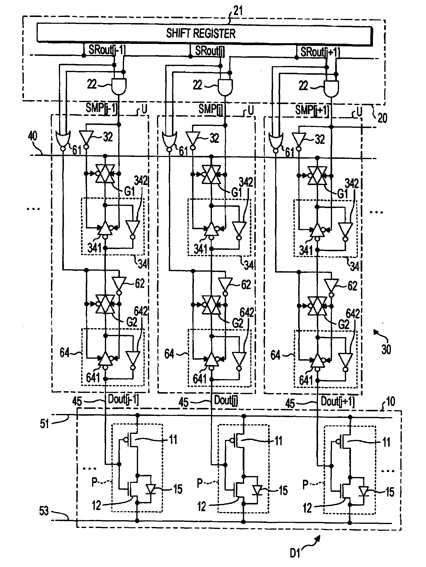
Figure 1 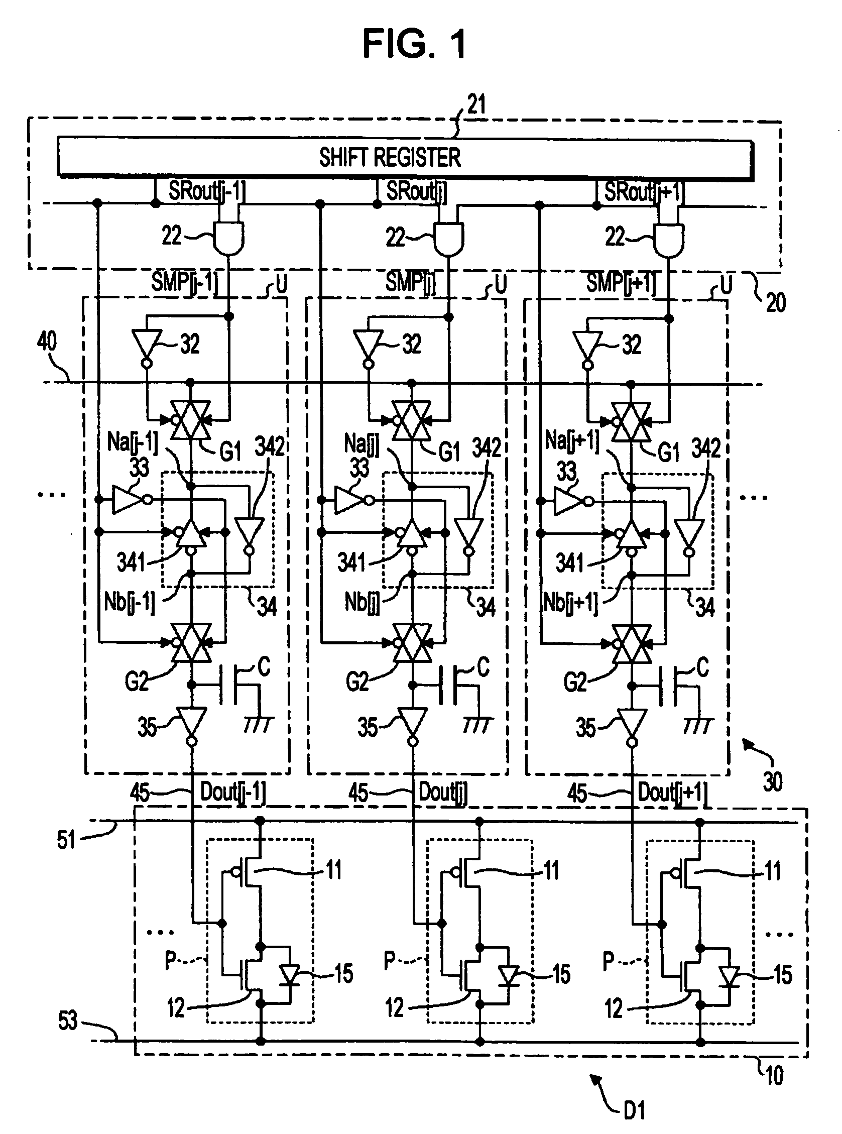
Figure 2 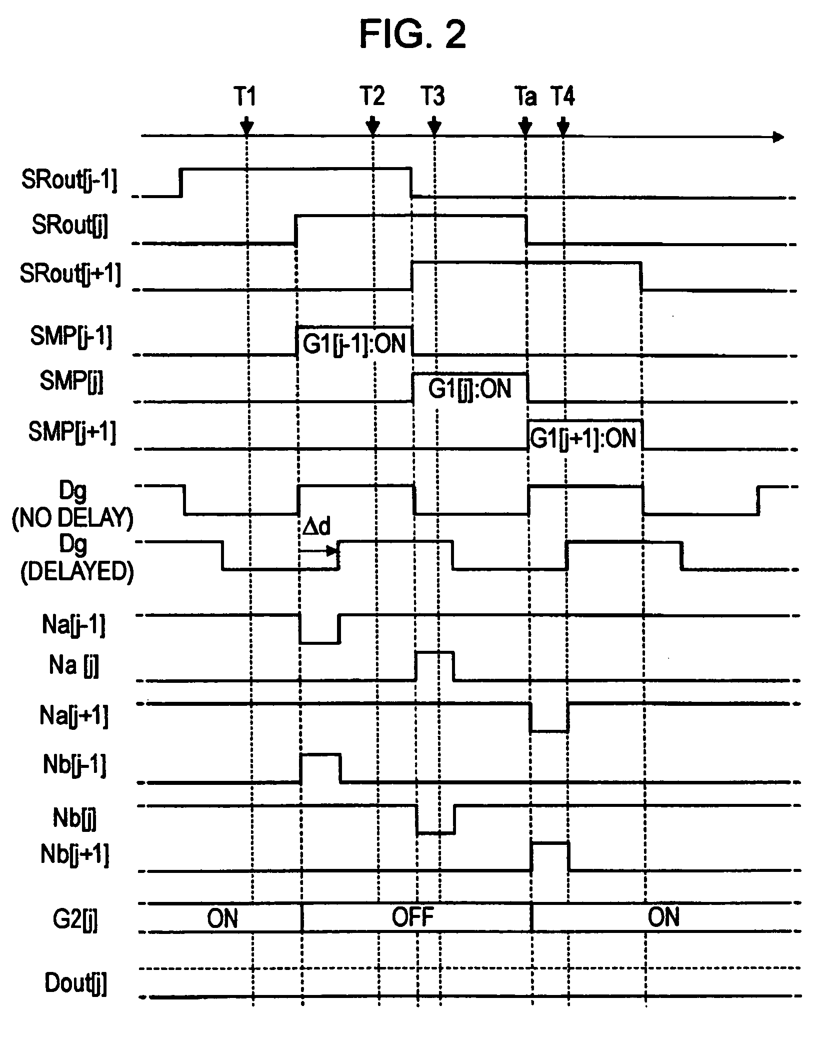
Figure 3
Abstract
Description
CROSS-REFERENCE TO RELATED APPLICATION
[0001] The present application claims priority to Japanese Patent Application No. 2005-011181 filed Jan. 19, 2005, which is hereby expressly incorporated by reference herein its entirety.BACKGROUND
[0002] 1. Technical Field
[0003] The present invention relates to a technology for controlling an electro-optical element such as an organic light-emitting diode (OLED) element or the like.
[0004] 2. Related Art
[0005] Generally, electro-optical devices with a plurality of electro-optical elements have been widely used. Each of the plurality of electro-optical elements is disposed so as to correspond to any one of a plurality of data lines, and a gray-scale level of each electro-optical element is controlled on the basis of a voltage applied to the corresponding data line. Each of the data lines is commonly connected to a signal line through a switching element disposed so as to correspond to the data line. This signal line is supplied with a gray-scale signal...
Examples
first embodiment
Modification of First Embodiment
[0058]Next, various modified aspects of the first embodiment will be described. Further, the various aspects of the first embodiment described below may be suitably combined. Hereinafter, in the various aspects, the same constituent elements as the first embodiment will be denoted by the same reference numerals as FIG. 1 and the description thereof will be omitted.
First Aspect
[0059]FIG. 5 is a circuit diagram showing a structure of the electro-optical device D1 according to the first aspect obtained by modifying the first embodiment. In FIG. 1, one end of the capacitor C is connected to a ground, but in the electro-optical device D1 according to the present aspect, one end of the capacitor C is connected to wiring lines including a wiring line to which a higher potential of a power supply Vdd is supplied (hereinafter, referred to as ‘higher power supply line’) and a wiring line to which a lower potential of a power supply Vss is supplied (hereinafter,...
second embodiment
Modification of Second Embodiment
[0071]Next, various modified aspects of the second embodiment will be described. Further, the various aspects of the second embodiment described below may be suitably combined. Hereinafter, in the various aspects, the same constituent elements as the first embodiment and the second embodiment will be described by the same reference numerals as FIGS. 1 and 10 and the description thereof will be omitted.
First Aspect
[0072]In FIG. 10, the voltage Dout of the data line 45 is held by only the gate capacitor Cg. However, one end of the same capacitor C as the first embodiment may be connected to the output terminal of the clocked inverter 38. The structure shown in FIG. 5 or 6 may be applied to the present embodiment. For example, as shown in FIG. 11, a structure may be used in which one end of the capacitor C is connected to a wring line for connecting a higher power supply line supplied with the higher potential of the power supply Vdd and a lower power s...