
Method of making a semiconductor chip assembly with chip and encapsulant grinding
a semiconductor chip and encapsulant technology, applied in semiconductor devices, semiconductor/solid-state device details, electrical apparatus, etc., can solve the problems of assembly unreliability, mechanical stress on the solder joints, thermal mechanical wear or creep of the solder joints, etc., to enhance mechanical support and protection, facilitate manufacturing, and enhance thermal dissipation from the chip
Patent Information
- Authority / Receiving Office
- US · United States
- Patent Type
- Patents(United States)
- Current Assignee / Owner
- Publication Date
- 2011-08-09
- Estimated Expiration
- Not applicable · inactive patent
Smart Images
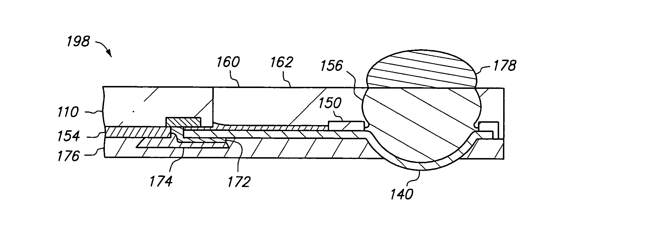
Figure 1 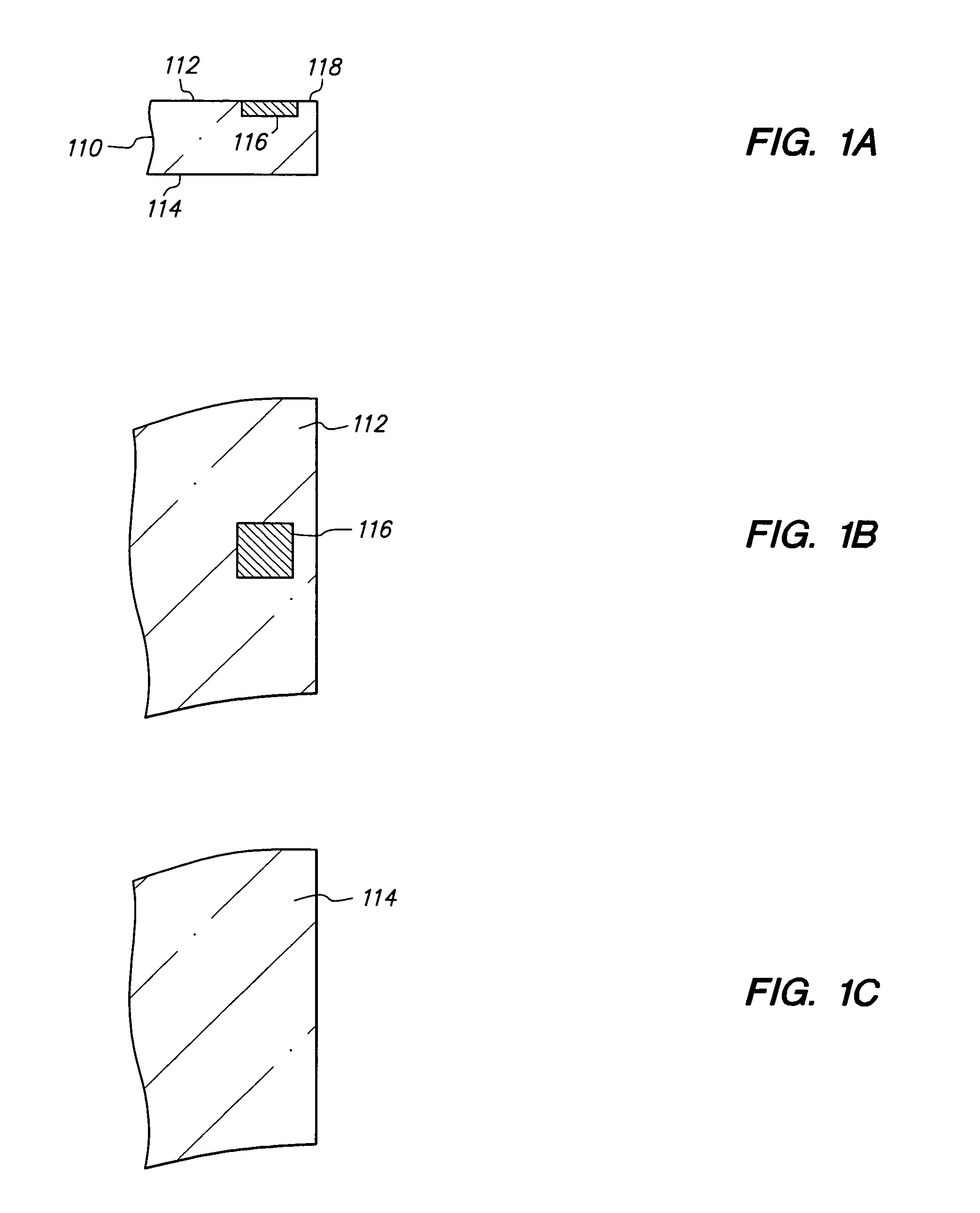
Figure 2 
Figure 3
Abstract
Description
CROSS-REFERENCE TO RELATED APPLICATIONS
[0001] This application is a continuation-in-part of U.S. application Ser. No. 11 / 498,614 filed Aug. 3, 2006 now U.S. Pat. No. 7,262,082, which is a continuation of U.S. application Ser. No. 10 / 971,856 filed Oct. 22, 2004 now U.S. Pat. No. 7,129,113, which is a continuation of U.S. application Ser. No. 10 / 966,816 filed Oct. 15, 2004 now U.S. Pat. No. 7,067,911, which is a continuation-in-part of U.S. application Ser. No. 10 / 922,280 filed Aug. 19, 2004 now U.S. Pat. No. 7,009,297, each of which is incorporated by reference.
[0002] This application is also a continuation-in-part of U.S. application Ser. No. 10 / 714,794 filed Nov. 17, 2003 now U.S. Pat. No. 7,190,080, which is incorporated by reference.BACKGROUND OF THE INVENTION
[0003] 1. Field of the Invention
[0004] The present invention relates to a semiconductor chip assembly, and more particularly to a semiconductor chip assembly with a chip and an encapsulant and its method of manufacture.
[0005] 2. ...
Examples
Embodiment Construction
[0057]FIGS. 1A-24A, 1B-24B and 1C-24C are cross-sectional, top and bottom views, respectively, of a method of making a semiconductor chip assembly in accordance with a first embodiment of the present invention.
[0058]FIGS. 1A, 1B and 1C are cross-sectional, top and bottom views, respectively, of semiconductor chip 110 which is an integrated circuit in which various transistors, circuits, interconnect lines and the like are formed (not shown). Chip 110 includes opposing major surfaces 112 and 114 and has a thickness (between surfaces 112 and 114) of 150 microns. Surface 112 is the active surface and includes conductive pad 116 and passivation layer 118.
[0059]Pad 116 is substantially aligned with passivation layer 118 so that surface 112 is essentially flat. Alternatively, if desired, pad 116 can extend above or be recessed below passivation layer 118. Pad 116 provides a bonding site to electrically couple chip 110 with external circuitry. Thus, pad 116 can be an input / output pad or a ...