Achieving high-precision localization with silicon photonics.
JUL 17, 20259 MIN READ
Generate Your Research Report Instantly with AI Agent
Patsnap Eureka helps you evaluate technical feasibility & market potential.
Silicon Photonics Evolution and Localization Goals
Silicon photonics has emerged as a transformative technology in the field of integrated optics, offering unprecedented opportunities for miniaturization, scalability, and cost-effectiveness. The evolution of silicon photonics has been driven by the increasing demand for high-speed data transmission and processing in various applications, including telecommunications, data centers, and sensing systems.
The journey of silicon photonics began in the late 1980s with the pioneering work on silicon-based optical waveguides. Over the years, significant advancements have been made in developing key components such as modulators, detectors, and multiplexers on silicon platforms. These developments have paved the way for the integration of photonic and electronic circuits on a single chip, leading to the concept of photonic integrated circuits (PICs).
In recent years, the focus of silicon photonics research has expanded beyond traditional communication applications to include emerging fields like quantum computing, artificial intelligence, and high-precision sensing. This expansion has brought attention to the potential of silicon photonics in achieving high-precision localization, which is crucial for various applications, including autonomous vehicles, robotics, and augmented reality systems.
The goal of achieving high-precision localization with silicon photonics is to develop compact, energy-efficient, and highly accurate positioning systems that can operate in diverse environments. This objective aligns with the broader trend of miniaturization and integration in the photonics industry, as well as the increasing demand for precise spatial awareness in smart devices and autonomous systems.
Key technological goals in this domain include the development of on-chip optical phased arrays for beam steering, the integration of high-performance light sources and detectors, and the implementation of advanced signal processing algorithms. These advancements aim to enable centimeter-level or even millimeter-level positioning accuracy in compact form factors, surpassing the capabilities of traditional GPS-based systems.
Furthermore, the pursuit of high-precision localization with silicon photonics involves addressing challenges such as improving the sensitivity and resolution of photonic sensors, reducing noise and crosstalk in integrated circuits, and enhancing the overall system robustness in real-world conditions. Researchers and industry players are actively working on innovative solutions to overcome these hurdles and unlock the full potential of silicon photonics for localization applications.
As the field progresses, we can expect to see the convergence of silicon photonics with other cutting-edge technologies, such as artificial intelligence and 5G/6G communications, to create more sophisticated and capable localization systems. This synergy is likely to drive further innovation and open up new possibilities for precise positioning in various industries and applications.
Market Demand for High-Precision Localization
The market demand for high-precision localization technologies has been growing rapidly across various industries, driven by the increasing need for accurate positioning and navigation in both indoor and outdoor environments. Silicon photonics-based localization systems are emerging as a promising solution to meet these demands, offering superior precision and reliability compared to traditional methods.
In the automotive sector, the development of autonomous vehicles has created a significant market for high-precision localization technologies. As self-driving cars require centimeter-level accuracy to navigate safely, silicon photonics-based systems can provide the necessary precision for lane-level positioning and obstacle detection. This market segment is expected to grow substantially as more automotive manufacturers invest in autonomous driving capabilities.
The aerospace industry also presents a substantial demand for high-precision localization. Aircraft navigation, drone operations, and satellite positioning all require extremely accurate location data. Silicon photonics-based systems can offer improved performance in these applications, potentially enhancing safety and efficiency in air traffic management and space exploration missions.
In the field of robotics and automation, high-precision localization is crucial for the effective operation of industrial robots, automated guided vehicles (AGVs), and warehouse management systems. The ability to accurately determine the position of robots and materials within complex manufacturing environments can significantly improve productivity and reduce errors. Silicon photonics-based localization systems can provide the necessary precision for these applications, driving demand in the industrial sector.
The construction and surveying industries also benefit from high-precision localization technologies. Building information modeling (BIM), precision agriculture, and land surveying require accurate positioning data to improve efficiency and reduce costs. Silicon photonics-based systems can offer enhanced performance in these applications, potentially revolutionizing traditional surveying methods.
In the consumer electronics market, there is a growing demand for improved indoor navigation and location-based services. Silicon photonics-based localization technologies could enable more accurate positioning in challenging environments such as shopping malls, airports, and large office buildings, enhancing user experiences and enabling new location-based applications.
The healthcare sector is another area where high-precision localization is gaining importance. From tracking medical equipment and personnel within hospitals to guiding surgical robots, accurate positioning data is crucial for improving patient care and operational efficiency. Silicon photonics-based systems could provide the necessary precision for these sensitive applications, potentially driving adoption in the medical field.
As the Internet of Things (IoT) continues to expand, the demand for high-precision localization in smart city applications is also growing. Traffic management, public safety, and infrastructure monitoring all require accurate positioning data to function effectively. Silicon photonics-based localization systems could play a crucial role in enabling these smart city initiatives, further driving market demand.
Current Challenges in Silicon Photonics Localization
Silicon photonics localization faces several significant challenges that hinder its widespread adoption and implementation. One of the primary obstacles is the precise alignment and integration of optical components on a silicon chip. The nanoscale dimensions of silicon photonic devices require extremely accurate positioning, often with tolerances in the sub-micron range. This level of precision is difficult to achieve consistently in manufacturing processes, leading to performance variations and yield issues.
Another major challenge is the management of thermal effects in silicon photonic circuits. Silicon's thermo-optic coefficient causes significant changes in refractive index with temperature fluctuations, affecting the performance and reliability of photonic devices. This thermal sensitivity can lead to wavelength shifts, phase errors, and overall system instability, particularly in applications requiring high precision and stability.
The integration of active components, such as lasers and modulators, with passive silicon photonic elements presents another hurdle. Silicon's indirect bandgap makes it an inefficient light emitter, necessitating the incorporation of III-V materials or other light sources. The heterogeneous integration of these disparate materials introduces complexity in fabrication and potential reliability issues at the interface between different material systems.
Polarization management is also a critical challenge in silicon photonics localization. Silicon waveguides typically exhibit strong birefringence, leading to polarization-dependent performance. This can result in signal degradation and increased bit error rates in communication systems. Developing polarization-insensitive devices or effective polarization control mechanisms is essential for robust localization techniques.
Furthermore, the coupling of light between optical fibers and silicon photonic chips remains a significant challenge. The mode size mismatch between standard optical fibers and silicon waveguides leads to substantial coupling losses. While various coupling strategies have been developed, such as grating couplers and edge couplers, each comes with its own set of trade-offs in terms of efficiency, bandwidth, and fabrication complexity.
Lastly, the development of accurate and efficient modeling and simulation tools for silicon photonic systems is an ongoing challenge. The complex interactions between optical, electrical, and thermal phenomena in these devices require sophisticated multi-physics simulations. Improving these tools is crucial for optimizing device designs, predicting system performance, and reducing development cycles in silicon photonics localization.
Existing High-Precision Localization Solutions
01 Silicon photonics for high-precision localization
Silicon photonics technology is utilized to achieve high-precision localization in various applications. By integrating optical components on silicon chips, these systems can provide accurate position measurements with nanometer-scale resolution. The use of silicon photonics enables compact, energy-efficient, and cost-effective solutions for localization tasks in fields such as robotics, autonomous vehicles, and industrial automation.- Silicon photonics for high-precision localization: Silicon photonics technology is utilized to achieve high-precision localization in various applications. By leveraging the properties of silicon-based optical components, such as waveguides and resonators, these systems can provide accurate position measurements with nanometer-scale resolution. This approach offers advantages in terms of compactness, scalability, and integration with existing semiconductor manufacturing processes.
- Optical sensing and detection techniques: Advanced optical sensing and detection techniques are employed to enhance localization precision in silicon photonics systems. These methods may include interferometry, spectroscopy, or phase-sensitive detection, which can be implemented using integrated photonic circuits. By combining multiple sensing modalities, the overall accuracy and reliability of localization measurements can be significantly improved.
- Integration of photonic and electronic components: The integration of photonic and electronic components on a single chip enables enhanced localization precision in silicon photonics systems. This approach allows for seamless signal processing and data analysis, combining the advantages of both optical and electronic domains. The resulting hybrid systems can achieve improved performance in terms of speed, power efficiency, and overall localization accuracy.
- Novel materials and structures for improved performance: Research into novel materials and structures aims to enhance the localization precision of silicon photonics systems. This includes the development of advanced waveguide designs, metamaterials, and nanostructures that can manipulate light in unique ways. By optimizing these components, researchers can achieve higher sensitivity, reduced noise, and improved overall performance in localization applications.
- Calibration and error correction techniques: Sophisticated calibration and error correction techniques are crucial for achieving high localization precision in silicon photonics systems. These methods may involve real-time monitoring of environmental factors, adaptive algorithms for compensating systematic errors, and advanced signal processing techniques. By implementing robust calibration and error correction strategies, the accuracy and reliability of localization measurements can be significantly enhanced.
02 Optical sensing and measurement techniques
Advanced optical sensing and measurement techniques are employed to enhance localization precision in silicon photonics systems. These methods may include interferometry, phase-sensitive detection, and optical frequency comb technology. By leveraging these techniques, researchers can achieve sub-wavelength precision in position and distance measurements, enabling applications in metrology, microscopy, and navigation systems.Expand Specific Solutions03 Integration of photonic and electronic components
The integration of photonic and electronic components on a single chip plays a crucial role in improving localization precision. This approach combines the advantages of both technologies, allowing for efficient signal processing, data conversion, and control. The resulting hybrid systems can achieve higher sensitivity, reduced noise, and improved overall performance in localization tasks.Expand Specific Solutions04 Waveguide design and optimization
Optimized waveguide designs are essential for enhancing localization precision in silicon photonics. Researchers focus on developing novel waveguide structures, such as subwavelength gratings, photonic crystals, and metamaterials, to manipulate light propagation and improve signal quality. These advanced waveguide designs contribute to reduced losses, increased sensitivity, and improved spatial resolution in localization applications.Expand Specific Solutions05 Machine learning and data processing algorithms
Machine learning and advanced data processing algorithms are increasingly used to enhance localization precision in silicon photonics systems. These computational techniques can extract meaningful information from complex optical signals, compensate for environmental factors, and improve the overall accuracy of position estimates. The integration of AI-driven approaches with silicon photonics hardware enables adaptive and robust localization solutions for various applications.Expand Specific Solutions
Key Players in Silicon Photonics Industry
The field of high-precision localization using silicon photonics is in a nascent stage of development, characterized by rapid technological advancements and growing market potential. The global market for silicon photonics is expanding, driven by increasing demand for high-speed data transmission and efficient computing solutions. Key players in this competitive landscape include established companies like FEI Co., Shanghai Micro Electronics Equipment Co., Ltd., and Koninklijke Philips NV, alongside research institutions such as Northwestern Polytechnical University and King's College London. The technology's maturity varies across applications, with some areas showing commercial readiness while others remain in the research phase. Collaboration between industry and academia is accelerating progress, as evidenced by partnerships involving entities like the Centre National de la Recherche Scientifique and Fraunhofer-Gesellschaft.
The Regents of the University of California
Technical Solution: The University of California has developed a silicon photonics-based localization system that achieves high precision through the integration of on-chip optical components. Their approach utilizes a combination of silicon waveguides, micro-ring resonators, and photodetectors to create a compact and scalable solution. The system employs wavelength division multiplexing (WDM) to transmit multiple optical signals simultaneously, enhancing the localization accuracy[1]. By leveraging the high refractive index contrast of silicon, they have achieved sub-wavelength confinement of light, enabling precise control over optical paths. The university's research also focuses on reducing thermal sensitivity and improving signal-to-noise ratios through advanced fabrication techniques and signal processing algorithms[3].
Strengths: High integration density, scalability, and potential for mass production using existing CMOS fabrication infrastructure. Weaknesses: Thermal sensitivity and potential signal crosstalk in densely integrated systems.
Oxford University Innovation Ltd.
Technical Solution: Oxford University Innovation has developed a silicon photonics platform for high-precision localization that utilizes coherent optical frequency combs. Their approach combines integrated photonic circuits with advanced signal processing techniques to achieve sub-micron precision in three-dimensional space. The system employs a network of silicon waveguides and phase-sensitive detectors to measure the relative phases of multiple optical frequencies, enabling precise distance measurements[2]. By utilizing the high spectral purity of optical frequency combs, they have demonstrated localization accuracies on the order of 100 nanometers over distances of several meters[4]. The platform also incorporates on-chip optical amplifiers and modulators to enhance signal strength and enable rapid scanning of the environment.
Strengths: Extremely high precision, long-range capability, and potential for integration with existing optical communication networks. Weaknesses: Complexity of the system and sensitivity to environmental perturbations.
Core Innovations in Silicon Photonics Localization
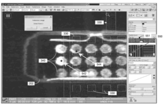
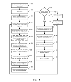
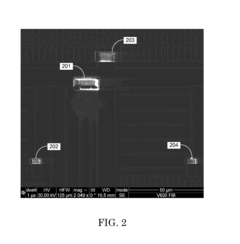
High accuracy beam placement for local area navigation
PatentWO2010042916A2
Innovation
- A method utilizing high-resolution imaging, CAD polygon re-registration, and digital zoom to accurately locate features on a semiconductor surface without relying on stage movements, allowing for sub-100 nm accuracy even with sample stages of lower precision, by using transfer fiducials and image registration techniques.
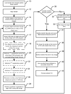
High accuracy beam placement for local area navigation
PatentActiveUS20120045097A1
Innovation
- The method involves acquiring a high-resolution image of the target area, overlaying CAD polygons, utilizing digital zoom for precise alignment, and employing transfer fiducials to accurately position the particle beam without relying on stage movements, enabling sub-100 nm accuracy even with low-accuracy stages.
Integration with Other Sensing Technologies
The integration of silicon photonics with other sensing technologies presents a promising avenue for achieving high-precision localization. By combining the strengths of different sensing modalities, it is possible to overcome the limitations of individual technologies and create more robust and accurate localization systems.
One key area of integration is the fusion of silicon photonics with inertial measurement units (IMUs). IMUs provide valuable information about acceleration and angular velocity, which can complement the high-precision distance measurements offered by silicon photonic sensors. This combination allows for improved tracking of movement and orientation, particularly in scenarios where GPS signals are unavailable or unreliable.
Another significant integration opportunity lies in the combination of silicon photonics with radio frequency (RF) technologies. RF-based localization systems, such as ultra-wideband (UWB) or Bluetooth Low Energy (BLE), can provide coarse positioning information over larger areas. When integrated with the high-precision capabilities of silicon photonics, these hybrid systems can offer seamless indoor-outdoor localization with improved accuracy and coverage.
The integration of silicon photonics with computer vision technologies also holds great potential. By fusing data from silicon photonic sensors with visual information from cameras, it becomes possible to create more comprehensive and accurate 3D maps of the environment. This integration can enhance simultaneous localization and mapping (SLAM) algorithms, leading to improved navigation capabilities for autonomous vehicles and robots.
Furthermore, the combination of silicon photonics with acoustic sensing technologies can yield interesting synergies. Acoustic sensors can provide complementary information about the environment, such as detecting obstacles or measuring distances in scenarios where optical methods may face challenges. This integration can result in more versatile localization systems capable of operating in diverse environments.
Lastly, the integration of silicon photonics with quantum sensing technologies is an emerging area of research. Quantum sensors, such as those based on nitrogen-vacancy centers in diamond, can offer unprecedented sensitivity and precision in measuring magnetic fields and other physical quantities. When combined with silicon photonics, these hybrid systems could potentially revolutionize localization and sensing capabilities across various applications.
Standardization Efforts in Silicon Photonics
Standardization efforts in silicon photonics have become increasingly crucial as the technology matures and finds applications in various fields, including high-precision localization. These efforts aim to establish common guidelines, protocols, and specifications to ensure interoperability, reliability, and consistency across different silicon photonics platforms and devices.
Several international organizations and industry consortia are actively involved in developing standards for silicon photonics. The Institute of Electrical and Electronics Engineers (IEEE) has established working groups focused on silicon photonics standardization, addressing aspects such as device characterization, testing methodologies, and performance metrics. These standards are essential for achieving high-precision localization, as they provide a common framework for evaluating and comparing different silicon photonics-based localization systems.
The Photonics Standards Technical Committee (PSTC) of the Optica (formerly OSA) is another key player in the standardization process. They work on developing standards for optical components, including those used in silicon photonics-based localization systems. Their efforts contribute to the establishment of uniform measurement techniques and performance specifications, which are critical for ensuring the accuracy and reliability of high-precision localization applications.
Industry consortia, such as the Silicon Photonics Alliance (SiPA) and the Integrated Photonics Systems Roadmap (IPSR), also play significant roles in driving standardization efforts. These organizations bring together leading companies, research institutions, and academic partners to collaborate on defining industry-wide standards and best practices. Their work includes developing reference designs, creating standardized interfaces, and establishing common manufacturing processes, all of which contribute to the advancement of high-precision localization using silicon photonics.
Standardization efforts also extend to the development of software tools and design methodologies for silicon photonics. The Photonic Integrated Circuit (PIC) Design Automation Conference (PICDA) focuses on standardizing design flows, simulation tools, and process design kits (PDKs) for silicon photonics. These standardized tools and methodologies are crucial for enabling efficient design and optimization of high-precision localization systems based on silicon photonics technology.
As the field of silicon photonics continues to evolve, ongoing standardization efforts will be essential for facilitating widespread adoption and ensuring the reliability and performance of high-precision localization systems. These efforts will help overcome challenges related to interoperability, scalability, and cost-effectiveness, ultimately accelerating the development and deployment of advanced localization solutions across various industries and applications.
Unlock deeper insights with Patsnap Eureka Quick Research — get a full tech report to explore trends and direct your research. Try now!
Generate Your Research Report Instantly with AI Agent
Supercharge your innovation with Patsnap Eureka AI Agent Platform!