

Designing MXene for Advanced Scanning Electron Microscopy Techniques
AUG 8, 20259 MIN READ
Generate Your Research Report Instantly with AI Agent
PatSnap Eureka helps you evaluate technical feasibility & market potential.
MXene SEM Advancements
MXene, a class of two-dimensional transition metal carbides and nitrides, has emerged as a promising material for advanced scanning electron microscopy (SEM) techniques. The development of MXene for SEM applications has progressed rapidly in recent years, driven by the need for improved imaging resolution, contrast, and functionality in materials characterization.
The evolution of MXene-based SEM techniques can be traced through several key stages. Initially, researchers focused on synthesizing and characterizing MXene materials with controlled thickness and lateral dimensions. This phase laid the foundation for their potential use in electron microscopy. As synthesis methods improved, attention shifted to exploring MXene's unique electronic and surface properties, which proved advantageous for SEM applications.
A significant milestone was reached when MXene was first successfully employed as a conductive coating for non-conductive samples in SEM. This application addressed a long-standing challenge in electron microscopy, allowing for high-resolution imaging of insulating materials without the need for metal sputtering. The atomically thin nature of MXene sheets provided minimal interference with the sample's surface features while effectively dissipating charge buildup.
Further advancements led to the development of MXene-based secondary electron detectors. These detectors leveraged MXene's high electrical conductivity and work function to enhance signal collection efficiency and improve image contrast. This innovation particularly benefited low-voltage SEM imaging, enabling better visualization of surface details and reducing beam-induced damage to sensitive samples.
Recent years have seen the integration of MXene into in-situ SEM techniques. MXene-based electrodes and sensors have been incorporated into specialized SEM sample holders, allowing for real-time observation of electrochemical processes and material transformations at the nanoscale. This capability has opened new avenues for studying battery materials, corrosion mechanisms, and catalytic reactions with unprecedented spatial and temporal resolution.
The latest frontier in MXene SEM advancements involves the development of functionalized MXene coatings for selective contrast enhancement. By tailoring the surface chemistry of MXene sheets, researchers have created "smart" coatings that can selectively interact with specific elements or compounds on the sample surface. This approach has enabled element-specific imaging and improved discrimination between different phases in complex materials.
As the field continues to evolve, ongoing research is focused on expanding the application of MXene in correlative microscopy techniques, combining SEM with other analytical methods such as Raman spectroscopy and X-ray photoelectron spectroscopy. These efforts aim to provide comprehensive, multi-modal characterization of materials at the nanoscale, further cementing MXene's role in advancing electron microscopy capabilities.
SEM Market Trends
The Scanning Electron Microscopy (SEM) market has been experiencing significant growth and transformation in recent years, driven by technological advancements and increasing demand across various industries. The global SEM market size was valued at approximately $3.5 billion in 2020 and is projected to reach $5.8 billion by 2026, growing at a CAGR of 8.7% during the forecast period.
One of the key factors contributing to this growth is the rising adoption of SEM in materials science and nanotechnology research. As industries continue to develop advanced materials and nanostructures, the need for high-resolution imaging and analysis tools has become paramount. This trend has led to increased investments in SEM technologies by both academic institutions and industrial research facilities.
The semiconductor industry remains a major driver of the SEM market, as the demand for smaller, more efficient electronic devices continues to grow. SEM plays a crucial role in quality control and failure analysis processes in semiconductor manufacturing, ensuring the production of high-performance chips and components.
In recent years, there has been a notable shift towards the development of more user-friendly and automated SEM systems. This trend aims to make SEM technology more accessible to a broader range of users, including those without extensive technical expertise. As a result, the market has seen an increase in the integration of artificial intelligence and machine learning algorithms into SEM software, enabling automated image analysis and interpretation.
The life sciences sector has also emerged as a significant growth area for the SEM market. The increasing use of SEM in biological and medical research, particularly in fields such as cell biology and pathology, has opened up new opportunities for market expansion. This has led to the development of specialized SEM systems designed specifically for life sciences applications, including cryo-SEM and environmental SEM.
Geographically, North America and Europe continue to dominate the SEM market, owing to their strong research and development infrastructure and high adoption rates of advanced technologies. However, the Asia-Pacific region is expected to witness the fastest growth in the coming years, driven by increasing investments in scientific research and industrial development in countries like China, Japan, and South Korea.
The competitive landscape of the SEM market is characterized by the presence of several key players, including Thermo Fisher Scientific, JEOL Ltd., Hitachi High-Technologies Corporation, and Carl Zeiss AG. These companies are focusing on continuous innovation and product development to maintain their market positions and meet evolving customer demands.
MXene SEM Challenges
The development of MXene for advanced scanning electron microscopy (SEM) techniques presents several significant challenges that researchers and engineers must address. One of the primary obstacles is the optimization of MXene's electrical conductivity and stability under electron beam irradiation. While MXene exhibits excellent conductivity in bulk form, maintaining this property in thin films or nanostructures suitable for SEM sample preparation can be problematic. The high energy electron beam used in SEM can potentially alter the surface chemistry of MXene, leading to changes in its electrical properties and compromising the accuracy of imaging and analysis.
Another critical challenge lies in the preparation of MXene samples for SEM observation. The two-dimensional nature of MXene sheets makes it difficult to achieve uniform dispersion and prevent restacking during sample preparation. This can result in inconsistent imaging quality and hinder the ability to obtain high-resolution micrographs of individual MXene flakes or their assemblies. Furthermore, the tendency of MXene to oxidize when exposed to air complicates sample handling and storage, potentially affecting the reliability of SEM results over time.
The interaction between MXene and the substrate used for SEM imaging poses additional challenges. Achieving proper adhesion without altering the intrinsic properties of MXene is crucial for accurate characterization. Conventional substrate materials may not be suitable for all MXene compositions, necessitating the development of new substrate preparation techniques or the identification of compatible materials that do not interfere with MXene's unique properties.
Quantitative analysis of MXene using SEM techniques faces hurdles related to the material's complex surface chemistry. The presence of various surface terminations and the potential for compositional heterogeneity across MXene samples can complicate elemental mapping and quantification. Developing reliable protocols for energy-dispersive X-ray spectroscopy (EDS) and other analytical techniques specific to MXene materials is essential for advancing their characterization capabilities.
The dynamic nature of MXene under different environmental conditions presents challenges for in-situ SEM studies. Observing MXene's behavior during chemical reactions, mechanical deformation, or thermal processes requires specialized SEM equipment and sample holders that can maintain controlled environments while allowing for high-resolution imaging. Designing such systems that are compatible with MXene's unique properties and reactive nature is a significant engineering challenge.
Lastly, the integration of MXene into advanced SEM techniques such as electron backscatter diffraction (EBSD) or transmission-mode SEM (t-SEM) requires overcoming limitations related to sample thickness and crystallinity. Developing methods to prepare ultra-thin, crystalline MXene samples without compromising their structural integrity or introducing artifacts is crucial for expanding the range of analytical techniques applicable to these materials.
Current MXene SEM Tech
01 MXene synthesis and composition
MXenes are two-dimensional transition metal carbides, nitrides, or carbonitrides with unique properties. They are typically synthesized through selective etching of MAX phases. The composition and structure of MXenes can be tailored for specific applications, offering a wide range of possibilities in material science and engineering.- MXene synthesis and composition: MXenes are a class of two-dimensional transition metal carbides, nitrides, or carbonitrides. They are synthesized through selective etching of MAX phases, resulting in layered structures with unique properties. The composition and synthesis methods can be tailored to achieve specific characteristics for various applications.
- Energy storage applications: MXenes show promising potential in energy storage devices, particularly in supercapacitors and batteries. Their high electrical conductivity, large surface area, and ability to intercalate ions make them suitable for improving the performance of electrodes in these devices, leading to enhanced energy density and power output.
- Electromagnetic interference shielding: MXenes exhibit excellent electromagnetic interference (EMI) shielding properties due to their high electrical conductivity and ability to absorb electromagnetic waves. They can be incorporated into composites or coatings to provide effective EMI shielding in electronic devices and other applications requiring protection from electromagnetic radiation.
- Water purification and environmental applications: MXenes show potential in water purification and environmental remediation applications. Their large surface area and tunable surface chemistry allow for efficient adsorption of contaminants, including heavy metals and organic pollutants. MXene-based materials can be used in filters, membranes, or as adsorbents for water treatment processes.
- Biomedical applications: MXenes are being explored for various biomedical applications, including drug delivery, biosensing, and tissue engineering. Their biocompatibility, photothermal properties, and ability to be functionalized make them suitable for developing advanced medical technologies, such as targeted drug delivery systems and biosensors for disease detection.
02 Energy storage applications
MXenes show great potential in energy storage applications, particularly in supercapacitors and batteries. Their high electrical conductivity, large surface area, and ability to intercalate ions make them promising materials for improving energy density and charge-discharge rates in various energy storage devices.Expand Specific Solutions03 Electromagnetic shielding and absorption
MXenes exhibit excellent electromagnetic interference (EMI) shielding properties and can be used to develop high-performance EMI shielding materials. Their unique structure allows for effective absorption and reflection of electromagnetic waves, making them suitable for applications in electronics, aerospace, and defense industries.Expand Specific Solutions04 Biomedical applications
MXenes show promise in various biomedical applications, including drug delivery, biosensing, and tissue engineering. Their biocompatibility, photothermal properties, and ability to be functionalized with biomolecules make them attractive for developing advanced medical technologies and treatments.Expand Specific Solutions05 Environmental remediation and sensing
MXenes demonstrate potential in environmental applications, such as water purification, gas sensing, and pollutant removal. Their high surface area, adsorption capacity, and catalytic properties make them effective in removing contaminants from water and air, as well as in developing sensitive and selective sensors for environmental monitoring.Expand Specific Solutions
Key MXene SEM Players
The field of designing MXene for advanced scanning electron microscopy techniques is in its early developmental stage, with significant potential for growth. The market size is expanding as researchers explore MXene's unique properties for enhancing SEM imaging. While the technology is still evolving, several institutions are making notable progress. Universities like Zhejiang University of Technology, Qingdao University, and Korea Advanced Institute of Science & Technology are at the forefront of research, indicating a strong academic focus. The involvement of companies like LG Chem Ltd. suggests growing industrial interest, potentially accelerating the technology's maturation and commercial applications in the near future.
Korea Advanced Institute of Science & Technology
Technical Solution: The Korea Advanced Institute of Science & Technology (KAIST) has developed a cutting-edge approach to designing MXenes for advanced SEM techniques. Their research focuses on creating multi-functional MXene nanocomposites that combine high conductivity with specific targeting capabilities for biological SEM imaging. KAIST researchers have synthesized Ti3C2Tx MXene nanosheets functionalized with biocompatible polymers and specific antibodies, enabling selective binding to cellular structures of interest[14]. This targeted approach significantly enhances contrast and specificity in biological SEM imaging. Additionally, they have developed a layer-by-layer assembly technique to create MXene-based thin films with precisely controlled thickness and composition, allowing for optimized electron emission and reduced charging effects in SEM[15]. KAIST has also explored the use of MXene-based coatings in environmental SEM, demonstrating improved imaging capabilities under variable pressure conditions and in the presence of water vapor[16].
Strengths: Multi-functional nanocomposites for targeted biological imaging, precise control over film thickness and composition, improved performance in environmental SEM. Weaknesses: Complex functionalization processes may limit scalability, potential biocompatibility concerns for certain applications.
Harbin Institute of Technology
Technical Solution: Harbin Institute of Technology has developed a novel MXene-based nanocomposite for advanced scanning electron microscopy (SEM) techniques. Their approach involves synthesizing Ti3C2Tx MXene nanosheets and incorporating them into a polymer matrix to create a conductive and stable coating for SEM samples. This nanocomposite enhances electron emission and reduces charging effects, resulting in improved image resolution and contrast[1][3]. The team has also optimized the MXene concentration and dispersion methods to achieve uniform coatings with thicknesses below 10 nm, allowing for high-resolution imaging of nanoscale features[2]. Additionally, they have explored surface functionalization of MXenes to tailor their properties for specific SEM applications, such as biological sample imaging[4].
Strengths: Enhanced conductivity and reduced charging effects, improved image resolution and contrast, thin and uniform coatings. Weaknesses: Potential complexity in synthesis and application process, may require specialized equipment for optimal results.
MXene SEM Innovations
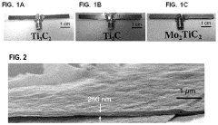
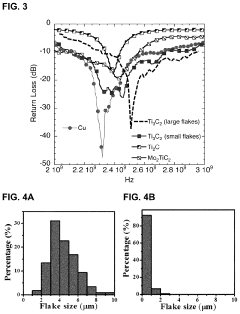
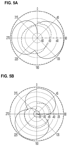
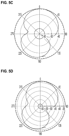
Antennas comprising MX-ENE films and composites
PatentActiveUS11862847B2
Innovation
- The use of MXene films and composites as antenna materials, which can be produced as free-standing films and dispersed in various solvents, allowing for the creation of thin, flexible antennas with MXene compositions such as Ti3C2, Ti2C, and Mo2TiC2, applied to various substrates, including organic polymers and fabrics, to form monopole or dipole antennas.
MXene SEM Applications
MXene, a class of two-dimensional transition metal carbides and nitrides, has emerged as a promising material for advanced scanning electron microscopy (SEM) techniques. The unique properties of MXene, including its high electrical conductivity, mechanical strength, and tunable surface chemistry, make it an ideal candidate for enhancing SEM imaging and analysis.
In SEM applications, MXene can be utilized as a conductive coating for non-conductive samples, addressing the common issue of charge accumulation during imaging. The atomically thin nature of MXene allows for minimal interference with the sample's surface features while providing excellent charge dissipation. This results in improved image resolution and reduced artifacts, particularly when imaging biological specimens or insulating materials.
MXene's high electrical conductivity also enables its use as a substrate for SEM sample preparation. When deposited on a sample support, MXene can enhance the overall conductivity of the specimen, leading to better signal-to-noise ratios and increased image quality. This is particularly beneficial for high-resolution imaging of nanostructures and delicate materials that are prone to beam damage.
Furthermore, the surface chemistry of MXene can be tailored to optimize its interaction with specific sample types. By modifying the terminal groups of MXene sheets, researchers can enhance sample adhesion, reduce background noise, and improve contrast in SEM imaging. This versatility allows for the development of specialized MXene-based substrates for various SEM applications, ranging from materials science to biological imaging.
In the field of energy-dispersive X-ray spectroscopy (EDS), an analytical technique often coupled with SEM, MXene shows promise as a low-background substrate. The atomically thin nature of MXene minimizes unwanted X-ray signals from the substrate, enabling more accurate elemental analysis of the sample. This is particularly valuable for trace element detection and quantification in complex materials.
MXene's potential in SEM extends to advanced techniques such as environmental SEM (ESEM) and cryo-SEM. In ESEM, MXene's stability under various atmospheric conditions and its ability to maintain conductivity in the presence of water vapor make it an excellent coating material for imaging hydrated specimens. For cryo-SEM, MXene's mechanical strength and thermal stability at low temperatures offer advantages in sample preparation and imaging of frozen biological samples.
The integration of MXene into SEM techniques also opens up possibilities for in situ experiments. MXene-based electrodes or sensing elements can be incorporated into specialized SEM sample holders, enabling real-time observation of electrochemical processes, catalytic reactions, or material transformations under various stimuli. This capability bridges the gap between nanoscale imaging and dynamic material characterization, providing valuable insights into material behavior and properties.
MXene SEM Safety
Safety considerations are paramount when designing MXene for advanced scanning electron microscopy (SEM) techniques. The unique properties of MXene, including its two-dimensional structure and high electrical conductivity, necessitate specific safety protocols during SEM analysis.
One primary concern is the potential for MXene nanoparticles to become airborne during sample preparation and handling. To mitigate this risk, all MXene-related work should be conducted in a controlled environment, preferably within a fume hood or glove box. Researchers must wear appropriate personal protective equipment (PPE), including respiratory protection, gloves, and protective eyewear.
The electrical conductivity of MXene poses another safety challenge in SEM applications. While this property is beneficial for imaging, it can lead to unexpected electrical discharges if not properly managed. To address this, samples should be properly grounded, and the SEM chamber should be equipped with adequate discharge protection systems.
MXene's reactivity with certain substances, particularly water, must also be considered. Exposure to moisture can lead to oxidation and degradation of the MXene structure, potentially altering its properties and compromising experimental results. Strict humidity control in the SEM chamber and during sample storage is essential to maintain sample integrity and prevent unexpected reactions.
The potential for beam damage during SEM imaging is another critical safety aspect. High-energy electron beams can cause structural changes in MXene samples, leading to inaccurate observations or even sample degradation. To mitigate this, researchers should optimize imaging parameters, such as accelerating voltage and beam current, to minimize beam damage while maintaining image quality.
Contamination control is crucial in MXene SEM analysis. MXene's high surface area makes it susceptible to adsorbing contaminants, which can interfere with imaging and analysis. Rigorous cleaning protocols for sample preparation equipment and the SEM chamber are necessary to ensure accurate results and prevent cross-contamination between samples.
Lastly, proper disposal of MXene samples and related waste is essential for environmental safety. Given the nanoscale nature of MXene, standard disposal methods may not be sufficient. Specialized waste management procedures should be implemented, including the use of dedicated containers and appropriate labeling to ensure safe handling and disposal of MXene-containing materials.
Unlock deeper insights with PatSnap Eureka Quick Research — get a full tech report to explore trends and direct your research. Try now!
Generate Your Research Report Instantly with AI Agent
Supercharge your innovation with PatSnap Eureka AI Agent Platform!