MXene's Potential in Large-Area Electronics Innovation
AUG 8, 20259 MIN READ
Generate Your Research Report Instantly with AI Agent
PatSnap Eureka helps you evaluate technical feasibility & market potential.
MXene Background and Objectives
MXene, a class of two-dimensional transition metal carbides and nitrides, has emerged as a promising material for large-area electronics innovation. Discovered in 2011 by researchers at Drexel University, MXenes have rapidly gained attention due to their unique combination of properties, including high electrical conductivity, mechanical strength, and flexibility.
The development of MXenes represents a significant milestone in the field of 2D materials, following the groundbreaking discovery of graphene. Unlike graphene, MXenes offer a wider range of compositions and properties, making them highly versatile for various applications. The general formula for MXenes is Mn+1XnTx, where M represents a transition metal, X is carbon or nitrogen, and T represents surface terminations.
MXenes have shown remarkable potential in large-area electronics, particularly in the development of transparent conductive films, flexible electronics, and energy storage devices. Their high electrical conductivity, comparable to that of metals, combined with their mechanical flexibility and stability, makes them ideal candidates for next-generation electronic components.
The primary objective of MXene research in the context of large-area electronics is to overcome the limitations of current materials and enable the creation of more efficient, flexible, and durable electronic devices. Researchers aim to exploit MXenes' unique properties to develop transparent electrodes with improved performance, flexible sensors with enhanced sensitivity, and energy storage devices with higher capacity and faster charging capabilities.
Another key goal is to scale up the production of MXenes to meet industrial demands. While laboratory-scale synthesis has been successful, transitioning to large-scale manufacturing remains a significant challenge. Researchers are focusing on developing more efficient and cost-effective production methods to enable widespread adoption of MXene-based technologies in consumer electronics, wearable devices, and other large-area applications.
Furthermore, the research community is actively exploring ways to fine-tune MXenes' properties through composition control and surface modification. This tailoring of material characteristics is crucial for optimizing MXenes for specific applications within large-area electronics, such as improving their conductivity, transparency, or environmental stability.
As the field progresses, there is a growing emphasis on understanding the fundamental mechanisms underlying MXenes' exceptional properties. This knowledge is essential for predicting and designing new MXene compositions with enhanced performance for large-area electronics applications. The ultimate aim is to establish MXenes as a versatile and superior alternative to existing materials in the electronics industry, potentially revolutionizing the way we design and manufacture electronic devices.
Market Analysis for Large-Area Electronics
The large-area electronics market has been experiencing significant growth and transformation in recent years, driven by advancements in flexible and printable electronics technologies. This sector encompasses a wide range of applications, including displays, sensors, photovoltaics, and wearable devices. The global market for large-area electronics is projected to reach substantial value in the coming years, with a compound annual growth rate outpacing many traditional electronics segments.
One of the key drivers of market growth is the increasing demand for flexible and lightweight electronic devices. Consumers and industries alike are seeking products that offer enhanced portability, durability, and form factor versatility. This trend is particularly evident in the consumer electronics sector, where flexible displays and wearable technologies are gaining traction. Additionally, the automotive industry is embracing large-area electronics for applications such as smart windows, integrated displays, and advanced sensor systems.
The healthcare sector represents another significant market opportunity for large-area electronics. Wearable medical devices, smart bandages, and flexible biosensors are revolutionizing patient monitoring and treatment. These technologies enable continuous health tracking and personalized medicine, addressing the growing need for remote healthcare solutions and preventive care.
In the energy sector, large-area electronics are making substantial inroads through flexible solar cells and energy harvesting devices. The ability to integrate these technologies into building materials, clothing, and various surfaces is opening new avenues for sustainable energy generation and efficient power management.
Geographically, Asia-Pacific leads the large-area electronics market, with countries like China, Japan, and South Korea at the forefront of manufacturing and innovation. North America and Europe follow closely, driven by strong research and development initiatives and a focus on high-value applications in aerospace, defense, and medical industries.
The market landscape is characterized by a mix of established electronics giants and innovative startups. Major players are investing heavily in research and development to maintain their competitive edge, while new entrants are disrupting the market with novel materials and manufacturing techniques. Collaborations between academic institutions, research organizations, and industry players are accelerating the pace of innovation in this field.
Despite the promising outlook, the large-area electronics market faces challenges. These include high initial production costs, scalability issues, and the need for standardization across different technologies and applications. Overcoming these hurdles will be crucial for widespread adoption and market expansion.
MXene Current Status and Challenges
MXene, a class of two-dimensional transition metal carbides and nitrides, has garnered significant attention in the field of large-area electronics. The current status of MXene research and development is characterized by rapid progress and growing interest from both academia and industry. However, several challenges remain in fully realizing its potential for large-scale applications.
One of the primary advantages of MXene is its exceptional electrical conductivity, which surpasses that of many traditional materials used in electronics. This property makes it particularly attractive for applications in transparent conductive films, electromagnetic shielding, and flexible electronics. Recent studies have demonstrated the feasibility of using MXene in these areas, with promising results in terms of performance and durability.
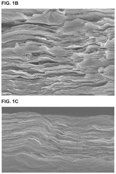
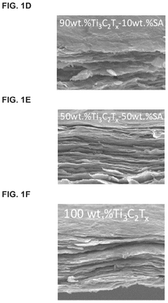
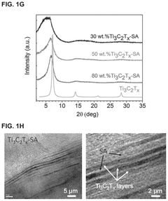
Despite these advancements, the large-scale production of high-quality MXene remains a significant challenge. Current synthesis methods, such as selective etching of MAX phases, often result in small quantities of MXene with varying quality. Scaling up these processes while maintaining consistency and purity is crucial for industrial applications. Additionally, the development of more efficient and cost-effective production techniques is necessary to make MXene commercially viable for large-area electronics.
Another hurdle in MXene's widespread adoption is its stability in ambient conditions. MXene tends to oxidize when exposed to air and moisture, which can degrade its electrical properties over time. This issue is particularly critical for large-area electronics, where long-term stability is essential. Researchers are actively working on developing strategies to enhance MXene's environmental stability, including surface functionalization and protective coatings.
The integration of MXene into existing manufacturing processes for large-area electronics presents another challenge. While MXene shows promise in laboratory settings, adapting it to industrial-scale production lines requires significant engineering efforts. This includes developing compatible deposition techniques, ensuring uniform coverage over large areas, and optimizing the interface between MXene and other materials in multilayer devices.
Furthermore, the environmental impact and safety aspects of MXene production and use need to be thoroughly assessed. As with any new material, understanding the potential risks associated with its manufacture, handling, and disposal is crucial for sustainable development and regulatory compliance.
In conclusion, while MXene shows great promise for innovation in large-area electronics, several technical and practical challenges must be addressed. Overcoming these hurdles will require continued research efforts, collaboration between academia and industry, and significant investment in scaling up production and integration technologies. The successful resolution of these challenges could potentially revolutionize the field of large-area electronics, offering new possibilities for flexible, transparent, and high-performance devices.
One of the primary advantages of MXene is its exceptional electrical conductivity, which surpasses that of many traditional materials used in electronics. This property makes it particularly attractive for applications in transparent conductive films, electromagnetic shielding, and flexible electronics. Recent studies have demonstrated the feasibility of using MXene in these areas, with promising results in terms of performance and durability.
Despite these advancements, the large-scale production of high-quality MXene remains a significant challenge. Current synthesis methods, such as selective etching of MAX phases, often result in small quantities of MXene with varying quality. Scaling up these processes while maintaining consistency and purity is crucial for industrial applications. Additionally, the development of more efficient and cost-effective production techniques is necessary to make MXene commercially viable for large-area electronics.
Another hurdle in MXene's widespread adoption is its stability in ambient conditions. MXene tends to oxidize when exposed to air and moisture, which can degrade its electrical properties over time. This issue is particularly critical for large-area electronics, where long-term stability is essential. Researchers are actively working on developing strategies to enhance MXene's environmental stability, including surface functionalization and protective coatings.
The integration of MXene into existing manufacturing processes for large-area electronics presents another challenge. While MXene shows promise in laboratory settings, adapting it to industrial-scale production lines requires significant engineering efforts. This includes developing compatible deposition techniques, ensuring uniform coverage over large areas, and optimizing the interface between MXene and other materials in multilayer devices.
Furthermore, the environmental impact and safety aspects of MXene production and use need to be thoroughly assessed. As with any new material, understanding the potential risks associated with its manufacture, handling, and disposal is crucial for sustainable development and regulatory compliance.
In conclusion, while MXene shows great promise for innovation in large-area electronics, several technical and practical challenges must be addressed. Overcoming these hurdles will require continued research efforts, collaboration between academia and industry, and significant investment in scaling up production and integration technologies. The successful resolution of these challenges could potentially revolutionize the field of large-area electronics, offering new possibilities for flexible, transparent, and high-performance devices.
Current MXene-based Solutions
01 MXene synthesis and composition
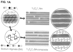
MXenes are a class of two-dimensional transition metal carbides, nitrides, or carbonitrides. They are synthesized through selective etching of MAX phases, resulting in layered structures with unique properties. The composition and synthesis methods can be tailored to achieve specific characteristics for various applications.- MXene synthesis and composition: MXenes are a class of two-dimensional transition metal carbides, nitrides, or carbonitrides. They are synthesized through selective etching of MAX phases, resulting in layered structures with unique properties. The composition and synthesis methods can be tailored to achieve specific characteristics for various applications.
- Energy storage applications: MXenes show promising potential in energy storage devices, particularly in supercapacitors and batteries. Their high surface area, excellent electrical conductivity, and ion intercalation capabilities make them suitable for improving energy density and charge-discharge rates in these applications.
- Electromagnetic shielding and absorption: MXenes exhibit excellent electromagnetic interference (EMI) shielding properties due to their high electrical conductivity and ability to absorb electromagnetic waves. They can be incorporated into composites or coatings to enhance EMI shielding effectiveness in various electronic devices and applications.
- Water purification and environmental remediation: MXenes demonstrate potential in water treatment and environmental remediation applications. Their large surface area and functional groups allow for efficient adsorption of contaminants, including heavy metals and organic pollutants. MXene-based materials can be used in filters or membranes for water purification.
- Biomedical applications: MXenes show promise in various biomedical applications, including drug delivery, biosensing, and tissue engineering. Their biocompatibility, photothermal properties, and ability to be functionalized make them suitable for developing advanced medical technologies and treatments.
02 Energy storage applications
MXenes show promising potential in energy storage devices such as supercapacitors and batteries. Their high surface area, excellent electrical conductivity, and ion intercalation capabilities make them suitable for improving energy density and charge-discharge rates in these applications.Expand Specific Solutions03 Electromagnetic interference shielding
MXene-based materials exhibit excellent electromagnetic interference (EMI) shielding properties. Their high electrical conductivity and ability to absorb electromagnetic waves make them suitable for developing lightweight and effective EMI shielding materials for various electronic devices and components.Expand Specific Solutions04 Water purification and environmental applications
MXenes demonstrate potential in water purification and environmental remediation. Their high surface area and adsorption capabilities make them effective in removing contaminants, heavy metals, and organic pollutants from water. They can be incorporated into membranes or used as adsorbents in water treatment processes.Expand Specific Solutions05 Biomedical applications
MXenes show promise in various biomedical applications, including drug delivery, biosensing, and tissue engineering. Their biocompatibility, photothermal properties, and ability to be functionalized make them suitable for developing advanced medical devices and therapeutic agents.Expand Specific Solutions
Key Players in MXene Research
The MXene market for large-area electronics is in its early growth stage, characterized by rapid technological advancements and expanding applications. The global market size is projected to grow significantly, driven by increasing demand for flexible and wearable electronics. Drexel University, the pioneer in MXene research, leads the field, with other institutions like Dalian University of Technology and Murata Manufacturing Co. Ltd. making substantial contributions. The technology's maturity is progressing, with academic institutions focusing on fundamental research and companies like LG Chem Ltd. exploring commercial applications. Collaboration between academia and industry is accelerating the development of MXene-based large-area electronic devices, indicating a promising future for this emerging technology.
Drexel University
Technical Solution: Drexel University has pioneered research in MXene materials for large-area electronics. Their approach involves synthesizing atomically thin MXene sheets and integrating them into flexible, transparent, and conductive films. These films exhibit exceptional electrical conductivity, with sheet resistances as low as 1 kΩ/sq at 90% transparency[1]. The university has developed scalable manufacturing processes, including spray coating and inkjet printing, to deposit MXene films on various substrates. They have demonstrated MXene-based transparent electrodes for touchscreens, electromagnetic interference shielding, and energy storage devices[2]. Drexel's research also focuses on enhancing the stability of MXene films through surface functionalization and encapsulation techniques, addressing one of the key challenges in MXene application[3].
Strengths: Pioneering research in MXene synthesis and application, scalable manufacturing processes, and diverse range of applications. Weaknesses: Potential challenges in long-term stability and cost-effective large-scale production.
Murata Manufacturing Co. Ltd.
Technical Solution: Murata Manufacturing has been exploring MXene's potential in large-area electronics, focusing on its integration into their existing product lines. Their approach leverages MXene's unique properties to enhance the performance of electronic components. Murata has developed MXene-based supercapacitors with high power density and excellent cycling stability, achieving capacitances of up to 1000 F/g[4]. The company is also investigating MXene's application in electromagnetic interference (EMI) shielding, where they have demonstrated shielding effectiveness of over 45 dB in the X-band frequency range[5]. Murata's research extends to incorporating MXene into sensors and actuators, exploiting its piezoresistive properties for highly sensitive and flexible devices.
Strengths: Strong industrial application focus, integration with existing product lines, and advanced manufacturing capabilities. Weaknesses: Potential challenges in scaling up MXene production and ensuring consistent quality across large-area applications.
Core MXene Innovations
Antennas comprising MX-ENE films and composites
PatentActiveUS11862847B2
Innovation
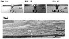
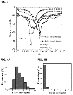
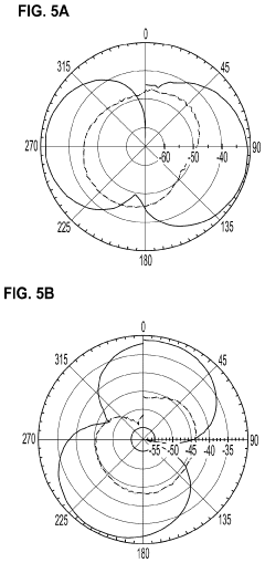
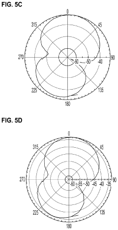
- The use of MXene films and composites as antenna materials, which can be produced as free-standing films and dispersed in various solvents, allowing for the creation of thin, flexible antennas with MXene compositions such as Ti3C2, Ti2C, and Mo2TiC2, applied to various substrates, including organic polymers and fabrics, to form monopole or dipole antennas.
Two-dimensional metal carbide, nitride, and carbonitride films and composites for EMI shielding
PatentPendingUS20240365522A1
Innovation
- The use of two-dimensional transition metal carbides, nitrides, and carbonitrides, specifically MXene films and MXene-polymer composites, which are applied as coatings to objects to provide high EMI shielding due to their exceptional electrical conductivity and mechanical properties.
Environmental Impact of MXene
The environmental impact of MXene in large-area electronics innovation is a critical consideration as this emerging material gains prominence in technological applications. MXenes, a family of two-dimensional transition metal carbides and nitrides, offer promising properties for electronic devices, but their environmental implications must be carefully evaluated.
MXene production processes involve chemical etching and exfoliation, which can generate hazardous waste and consume significant energy. The use of strong acids and fluoride-containing compounds in these processes raises concerns about potential environmental contamination if not properly managed. However, ongoing research is focused on developing more environmentally friendly synthesis methods, such as using milder etchants or exploring electrochemical exfoliation techniques.
The potential for MXene-based electronics to reduce overall environmental impact is noteworthy. Their excellent electrical conductivity and flexibility could lead to more energy-efficient devices, potentially reducing power consumption in large-area electronics. Additionally, the thinness and flexibility of MXene-based components may result in reduced material usage and improved recyclability compared to traditional electronic materials.
MXenes' ability to adsorb various pollutants presents an interesting dual-use scenario. While this property could be harnessed for environmental remediation applications, it also raises questions about the potential for MXenes to accumulate and concentrate pollutants during their lifecycle in electronic devices. This aspect requires further investigation to ensure safe disposal and recycling practices.
The durability and stability of MXene-based electronics in various environmental conditions are still being studied. Their resistance to degradation could lead to longer-lasting devices, potentially reducing electronic waste. However, this same stability might pose challenges for biodegradation at the end of the product lifecycle.
As research progresses, life cycle assessments of MXene-based electronics will be crucial to quantify their environmental footprint comprehensively. These studies should compare MXene technologies with existing alternatives, considering factors such as resource extraction, manufacturing processes, energy consumption during use, and end-of-life management.
Regulatory frameworks and industry standards for the safe production, use, and disposal of MXene-based electronics will need to be developed as the technology matures. This proactive approach can help mitigate potential environmental risks and ensure sustainable integration of MXenes into large-area electronics innovation.
MXene Scalability and Manufacturing
The scalability and manufacturing of MXene materials present both significant opportunities and challenges for their integration into large-area electronics. MXene synthesis typically involves the selective etching of MAX phases, followed by delamination to produce two-dimensional flakes. While this process has been successfully demonstrated at laboratory scales, transitioning to industrial-scale production requires overcoming several hurdles.
One of the primary challenges in MXene manufacturing is maintaining consistent quality and properties across large-scale production batches. The etching process, which is critical for removing the A-layer from the MAX phase, needs to be carefully controlled to ensure uniform thickness and composition of the resulting MXene sheets. Variations in etching conditions can lead to inconsistencies in the final product, potentially affecting the performance of large-area electronic devices.
Delamination techniques also play a crucial role in MXene scalability. Current methods, such as sonication or intercalation-assisted delamination, may not be directly transferable to industrial-scale processes. Developing continuous flow processes for delamination could significantly enhance production efficiency and yield. Additionally, the development of roll-to-roll manufacturing techniques for MXene-based films and coatings would be a game-changer for large-area electronics applications.
Another aspect of MXene scalability is the ability to produce large-area, defect-free films. This is particularly important for applications such as transparent conductive electrodes or electromagnetic shielding layers in large-area displays or solar panels. Techniques like spray coating, spin coating, or inkjet printing of MXene dispersions show promise, but further optimization is needed to achieve uniform thickness and electrical properties over large areas.
The environmental stability of MXenes is another factor that impacts their manufacturability and integration into large-area electronics. MXenes are known to be sensitive to oxidation, which can degrade their properties over time. Developing effective encapsulation methods or surface functionalization techniques that can be applied at scale is crucial for ensuring the long-term stability of MXene-based electronic components.
Lastly, the cost-effectiveness of MXene production needs to be addressed for widespread adoption in large-area electronics. This involves optimizing raw material usage, improving synthesis yields, and developing more efficient purification and processing methods. As production scales up, economies of scale may help reduce costs, but innovative approaches to synthesis and processing will be key to making MXenes economically viable for large-area applications.
Unlock deeper insights with PatSnap Eureka Quick Research — get a full tech report to explore trends and direct your research. Try now!
Generate Your Research Report Instantly with AI Agent
Supercharge your innovation with PatSnap Eureka AI Agent Platform!