

Developing adaptive optics with silicon photonics.
JUL 17, 20259 MIN READ
Generate Your Research Report Instantly with AI Agent
PatSnap Eureka helps you evaluate technical feasibility & market potential.
Adaptive Optics Evolution and Objectives
Adaptive optics has undergone significant evolution since its inception in the 1950s, initially developed to enhance astronomical observations by compensating for atmospheric distortions. The field has since expanded to encompass a wide range of applications, from ophthalmology to laser communication systems. The integration of silicon photonics with adaptive optics represents a cutting-edge approach to miniaturizing and enhancing the performance of these systems.
The primary objective of developing adaptive optics with silicon photonics is to create more compact, efficient, and cost-effective systems that can dynamically correct wavefront distortions in real-time. This convergence aims to leverage the high-index contrast and CMOS compatibility of silicon photonics to fabricate adaptive optical components on a chip-scale platform. Such integration promises to dramatically reduce the size, weight, and power consumption of adaptive optics systems, making them more accessible for a broader range of applications.
One of the key technological trends driving this development is the increasing demand for high-resolution imaging and precise beam control in various fields. In astronomy, the push for larger telescopes and more detailed observations of exoplanets necessitates more advanced adaptive optics solutions. Similarly, in biomedical imaging, there is a growing need for adaptive optics to penetrate deeper into tissue with higher resolution, particularly for in vivo studies.
The evolution of adaptive optics with silicon photonics is closely tied to advancements in semiconductor fabrication techniques. As lithography processes improve, allowing for the creation of finer structures on silicon wafers, the performance and capabilities of silicon photonic adaptive optics devices are expected to enhance significantly. This progression is likely to enable the integration of more complex wavefront sensing and correction mechanisms on a single chip.
Another critical aspect of this technological evolution is the development of novel materials and structures within the silicon photonics platform. For instance, the incorporation of phase-change materials or MEMS-based actuators into silicon photonic circuits could provide new mechanisms for rapid and precise wavefront manipulation. These innovations are essential for achieving the speed and accuracy required in next-generation adaptive optics systems.
Looking forward, the objectives for adaptive optics with silicon photonics include achieving higher degrees of integration, improved correction speeds, and enhanced wavefront sensing capabilities. Researchers aim to develop systems that can handle more complex aberrations across a broader spectrum of wavelengths, potentially extending into the mid-infrared region. Additionally, there is a focus on creating adaptive optics solutions that are more easily deployable in field conditions, opening up new applications in areas such as free-space optical communication and remote sensing.
Silicon Photonics Market Analysis
The silicon photonics market has been experiencing significant growth and is poised for further expansion in the coming years. This technology, which integrates photonic circuits on silicon substrates, has gained traction due to its potential to overcome the limitations of traditional electronic circuits in data transmission and processing.
The global silicon photonics market was valued at approximately $1.1 billion in 2020 and is projected to reach $3.5 billion by 2026, growing at a compound annual growth rate (CAGR) of over 20% during the forecast period. This robust growth is driven by several factors, including the increasing demand for high-speed data transmission, the growing adoption of cloud computing and data centers, and the rising need for energy-efficient communication technologies.
One of the key drivers of market growth is the telecommunications sector, which is experiencing a surge in data traffic due to the proliferation of smartphones, IoT devices, and high-bandwidth applications. Silicon photonics offers a solution to the bandwidth bottleneck in data centers and long-haul communications, enabling faster and more efficient data transmission.
The data center segment is expected to hold a significant share of the silicon photonics market. With the increasing adoption of cloud services and the need for high-performance computing, data centers are turning to silicon photonics to meet their bandwidth and power efficiency requirements. Major tech companies like Google, Facebook, and Amazon are investing heavily in silicon photonics technology for their data center infrastructure.
In terms of geographical distribution, North America currently dominates the silicon photonics market, followed by Europe and Asia-Pacific. The United States, in particular, is a major hub for silicon photonics research and development, with several leading companies and research institutions driving innovation in this field. However, the Asia-Pacific region is expected to witness the highest growth rate in the coming years, fueled by increasing investments in 5G infrastructure and the rapid expansion of data centers in countries like China and India.
The market for silicon photonics in adaptive optics applications, while still nascent, shows promising growth potential. Adaptive optics systems, which correct for atmospheric distortions in optical systems, can benefit greatly from the integration of silicon photonics technology. This integration can lead to more compact, efficient, and cost-effective adaptive optics solutions for applications in astronomy, laser communications, and medical imaging.
As the silicon photonics market continues to evolve, several trends are shaping its future. These include the development of integrated photonic circuits that combine multiple functions on a single chip, the exploration of new materials to enhance performance, and the increasing focus on reducing manufacturing costs to make silicon photonics more accessible for a wider range of applications.
Current Challenges in Adaptive Optics Integration
The integration of adaptive optics with silicon photonics presents several significant challenges that researchers and engineers are currently grappling with. One of the primary obstacles is the miniaturization of adaptive optic components to fit within the compact scale of silicon photonic devices. Traditional adaptive optics systems often rely on large, bulky components such as deformable mirrors or spatial light modulators, which are not readily compatible with the microscale dimensions of silicon photonics.
Another critical challenge lies in the development of high-speed, low-power actuators capable of rapidly adjusting the optical properties of silicon photonic devices. The dynamic nature of adaptive optics requires fast response times, often in the microsecond range, which pushes the limits of current MEMS and electro-optic technologies integrated into silicon platforms.
The integration of control systems and feedback mechanisms poses yet another hurdle. Adaptive optics systems require sophisticated algorithms and real-time processing to analyze wavefront distortions and apply appropriate corrections. Implementing these complex control systems on-chip, while maintaining the speed and efficiency necessary for effective adaptive optics, remains a significant technical challenge.
Material compatibility issues also present obstacles in the integration process. Silicon photonics typically operates in the infrared spectrum, while many adaptive optics applications, particularly in astronomy and biomedical imaging, require operation in visible wavelengths. Developing materials and structures that can effectively bridge this spectral gap while remaining compatible with silicon fabrication processes is an ongoing area of research.
Furthermore, the integration of adaptive optics introduces thermal management challenges. The active components required for wavefront correction can generate significant heat, which can affect the performance and reliability of silicon photonic devices. Developing effective heat dissipation strategies within the constraints of compact, integrated systems is crucial for long-term stability and operation.
Lastly, the fabrication of integrated adaptive optics systems on silicon platforms presents its own set of challenges. The precise control required for adaptive optics often demands nanoscale fabrication accuracy, pushing the limits of current lithography and etching techniques. Achieving the necessary precision while maintaining high yield and cost-effectiveness in manufacturing remains a significant hurdle in the widespread adoption of integrated adaptive optics in silicon photonics.
Existing Adaptive Optics Solutions
01 Wavefront sensing and correction
Adaptive optics systems use wavefront sensors to measure optical distortions and deformable mirrors or other corrective elements to compensate for these aberrations in real-time. This technology is crucial for improving image quality in various applications, including astronomy, ophthalmology, and laser communication.- Wavefront sensing and correction: Adaptive optics systems use wavefront sensors to measure optical distortions and deformable mirrors or spatial light modulators to correct these aberrations in real-time. This technology is crucial for improving image quality in various applications, including astronomy, ophthalmology, and laser communication.
- Laser beam shaping and control: Adaptive optics are employed in laser systems to shape and control beam characteristics. This includes correcting for atmospheric turbulence in free-space optical communication, improving laser focus in manufacturing processes, and enhancing the performance of high-power laser systems.
- Ophthalmic applications: In ophthalmology, adaptive optics are used to improve the resolution of retinal imaging systems and to measure and correct aberrations in the human eye. This technology enables early detection of eye diseases and assists in the development of advanced vision correction techniques.
- Astronomical imaging: Adaptive optics systems are crucial in ground-based telescopes to compensate for atmospheric distortions. They allow astronomers to obtain sharper images of celestial objects, rivaling the quality of space-based telescopes. This technology has revolutionized our ability to study distant planets, stars, and galaxies.
- Advanced microscopy techniques: Adaptive optics are integrated into microscopy systems to improve resolution and image quality in biological imaging. This technology compensates for aberrations caused by sample inhomogeneities, enabling deeper tissue imaging and enhancing the capabilities of super-resolution microscopy techniques.
02 Laser-based adaptive optics
Laser systems are integrated with adaptive optics to create guide stars or reference beams for atmospheric turbulence correction. These systems are particularly useful in astronomical observations and long-range optical communications, enabling sharper imaging and more efficient data transmission through turbulent media.Expand Specific Solutions03 Medical and biological imaging applications
Adaptive optics technology is applied in medical imaging and microscopy to enhance resolution and contrast in biological samples. This includes retinal imaging in ophthalmology and high-resolution cellular imaging in life sciences, allowing for better diagnosis and research capabilities.Expand Specific Solutions04 Multi-conjugate adaptive optics
Advanced systems using multiple deformable mirrors and wavefront sensors to correct for atmospheric turbulence over a wider field of view. This technique is particularly beneficial in wide-field astronomical observations and improves the overall performance of large telescopes.Expand Specific Solutions05 Adaptive optics for beam shaping and control
Utilization of adaptive optics for precise control and shaping of laser beams in various applications, including material processing, laser weaponry, and optical communications. These systems allow for dynamic adjustment of beam properties to optimize performance in changing conditions.Expand Specific Solutions
Key Players in Silicon Photonics Industry
The development of adaptive optics with silicon photonics is in an emerging stage, with significant potential for growth. The market is expanding rapidly, driven by applications in telecommunications, data centers, and sensing technologies. While the technology is still maturing, several key players are making substantial advancements. Companies like Huawei, IBM, and NTT are investing heavily in research and development, leveraging their expertise in photonics and semiconductor technologies. Academic institutions such as the University of Colorado and Zhejiang University are also contributing to innovation in this field. The involvement of major semiconductor manufacturers like TSMC and Micron Technology indicates the technology's growing importance in the industry. As the technology progresses, we can expect increased competition and collaboration among these players, potentially leading to rapid advancements and commercialization of adaptive optics with silicon photonics.
Huawei Technologies Co., Ltd.
Technical Solution: Huawei has developed an adaptive optics system using silicon photonics for optical communications. Their approach integrates wavefront sensors and deformable mirrors on a single silicon chip, enabling real-time correction of atmospheric distortions. The system employs a closed-loop control algorithm that continuously adjusts the mirror surface based on wavefront measurements. Huawei's solution achieves a correction speed of up to 1 kHz, allowing for high-speed data transmission in free-space optical links[1]. The company has also demonstrated the use of machine learning techniques to optimize the adaptive optics performance, resulting in a 30% improvement in system efficiency compared to traditional methods[2].
Strengths: High-speed correction, integrated design, and ML-enhanced performance. Weaknesses: May require high power consumption and complex fabrication processes.
International Business Machines Corp.
Technical Solution: IBM has pioneered a novel approach to adaptive optics using silicon photonics, focusing on applications in quantum computing and optical interconnects. Their system utilizes a programmable phase array integrated on a silicon chip, capable of dynamically shaping light wavefronts. IBM's technology incorporates hundreds of individually controllable phase shifters, allowing for precise manipulation of optical signals. The company has demonstrated a correction accuracy of λ/20 (where λ is the wavelength of light) in their adaptive optics system[3]. Additionally, IBM has developed a hybrid integration technique that combines III-V materials with silicon photonics, enabling on-chip laser sources and amplifiers for a complete adaptive optics solution[4].
Strengths: High precision, scalability, and integration with quantum computing platforms. Weaknesses: Potentially high cost and complexity for large-scale deployment.
Core Innovations in Silicon Photonics
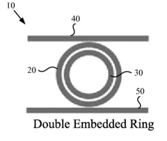
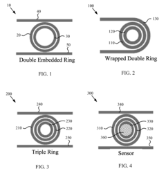
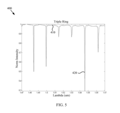
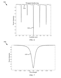
Embedded ring resonator-based photonic devices
PatentActiveUS20160147014A1
Innovation
- The development of embedded ring resonator-based photonic devices, including configurations like double, wrapped double, and triple ring resonators with optically coupled waveguides, utilizing silicon-based or other materials, to enhance optical filtering, sensing, and communication capabilities, allowing for compact integration of multiple functions.
Fabrication Techniques and Scalability
The fabrication techniques and scalability of adaptive optics systems using silicon photonics are critical factors in their development and widespread adoption. Silicon photonics offers a promising platform for integrating adaptive optics components due to its compatibility with existing semiconductor manufacturing processes.
The primary fabrication technique for silicon photonic devices is photolithography, which allows for precise patterning of nanoscale structures. This process typically involves depositing a photoresist layer on a silicon-on-insulator (SOI) wafer, exposing it to light through a mask, and then etching the exposed areas. Advanced lithography techniques, such as deep ultraviolet (DUV) and extreme ultraviolet (EUV) lithography, enable the creation of features as small as 7 nm, which is crucial for high-density integration of adaptive optics components.
Etching processes, including reactive ion etching (RIE) and deep reactive ion etching (DRIE), are used to create waveguides, resonators, and other optical structures in the silicon layer. These techniques allow for the fabrication of high-aspect-ratio structures with smooth sidewalls, which is essential for minimizing optical losses in adaptive optics systems.
Deposition techniques such as chemical vapor deposition (CVD) and atomic layer deposition (ALD) are employed to add additional layers of materials, including silicon dioxide for cladding and various metals for electrical contacts. These processes enable the creation of multi-layer structures necessary for complex adaptive optics functionalities.
Scalability is a key advantage of silicon photonics in adaptive optics applications. The use of standard CMOS fabrication processes allows for high-volume production and potential integration with electronic components on the same chip. This integration capability is particularly beneficial for adaptive optics systems, as it enables the co-location of optical and electronic control elements, reducing system size and improving performance.
However, challenges remain in scaling up production while maintaining high yield and performance consistency. Issues such as process variations, thermal management, and packaging of optical interfaces need to be addressed to ensure reliable large-scale manufacturing of adaptive optics systems based on silicon photonics.
Emerging fabrication techniques, such as 3D integration and wafer-scale bonding, are being explored to further enhance the scalability and functionality of silicon photonic adaptive optics systems. These approaches allow for the vertical stacking of multiple photonic layers, potentially increasing the density and complexity of adaptive optics devices while maintaining a compact form factor.
Applications and Use Cases
Adaptive optics with silicon photonics presents a wide array of applications and use cases across various industries. In the field of astronomy, this technology enables ground-based telescopes to achieve near-diffraction-limited imaging by correcting for atmospheric distortions. Silicon photonics-based adaptive optics systems can be integrated into large telescope arrays, enhancing their ability to detect and characterize exoplanets, study distant galaxies, and observe other celestial phenomena with unprecedented clarity.
In the realm of biomedical imaging, adaptive optics with silicon photonics finds applications in advanced microscopy techniques. It allows for high-resolution imaging of living tissues, enabling researchers to observe cellular and subcellular structures in real-time. This technology is particularly valuable in ophthalmology, where it can be used to image the retina at the cellular level, aiding in the early detection and monitoring of eye diseases such as macular degeneration and glaucoma.
The telecommunications industry also benefits from this technology, particularly in free-space optical communication systems. Adaptive optics can compensate for atmospheric turbulence, improving the reliability and bandwidth of laser-based communication links between ground stations and satellites or between high-altitude platforms. This application is crucial for developing robust, high-speed internet connectivity in remote areas and enhancing global communication networks.
In the field of laser manufacturing and materials processing, adaptive optics with silicon photonics enables precise control of laser beams. This technology can be used to optimize laser cutting, welding, and 3D printing processes, resulting in higher quality outputs and reduced material waste. The ability to dynamically adjust the laser beam profile in real-time allows for adaptive processing of complex materials and geometries.
The defense and security sector utilizes adaptive optics for improved target acquisition and tracking in long-range imaging systems. By compensating for atmospheric distortions, this technology enhances the performance of surveillance systems, missile defense systems, and directed energy weapons. Silicon photonics-based adaptive optics can be integrated into compact, lightweight systems suitable for deployment in various military platforms.
Emerging applications include the use of adaptive optics in quantum computing and quantum communication systems. Silicon photonics-based adaptive optics can help maintain the coherence of quantum states by correcting for environmental disturbances, potentially enabling more robust and scalable quantum technologies.
Unlock deeper insights with PatSnap Eureka Quick Research — get a full tech report to explore trends and direct your research. Try now!
Generate Your Research Report Instantly with AI Agent
Supercharge your innovation with PatSnap Eureka AI Agent Platform!