

Electride Interfaces With 2D Materials For Heterostructures
AUG 28, 20259 MIN READ
Generate Your Research Report Instantly with AI Agent
PatSnap Eureka helps you evaluate technical feasibility & market potential.
Electride-2D Materials Interface Background and Objectives
Electride materials represent a unique class of compounds where electrons serve as anions, occupying structural cavities rather than being bound to specific atoms. This distinctive electronic configuration endows electrides with exceptional properties, including high electron mobility, low work function, and remarkable catalytic activity. The integration of electrides with two-dimensional (2D) materials presents a frontier research area with immense potential for next-generation electronic and optoelectronic devices.
The evolution of electride research traces back to the 1980s with the pioneering work of James L. Dye on alkali metal electrides. However, these early electrides were unstable under ambient conditions, limiting their practical applications. A significant breakthrough occurred in 2003 with the discovery of the first room-temperature stable electride, 12CaO·7Al₂O₃ (C12A7:e⁻), by Hosono's group. This discovery catalyzed extensive research into electride materials and their potential applications.
Concurrently, the field of 2D materials has experienced explosive growth since the isolation of graphene in 2004. The atomically thin nature of 2D materials, coupled with their diverse electronic properties ranging from metals to semiconductors and insulators, offers unprecedented opportunities for designing novel heterostructures with tailored functionalities.
The convergence of electrides and 2D materials represents a natural progression in materials science, driven by the complementary properties of these two material classes. Electrides provide abundant free electrons and unique electronic structures, while 2D materials offer atomically precise interfaces and tunable electronic properties. The interface between these materials creates a rich playground for exploring novel physical phenomena and developing innovative device architectures.
The primary objectives of research in electride-2D material interfaces include understanding the fundamental interfacial charge transfer mechanisms, engineering band alignment for optimal device performance, and exploiting the unique properties of electrides to enhance the functionality of 2D material-based devices. Additionally, researchers aim to develop scalable fabrication techniques for creating high-quality electride-2D material heterostructures suitable for commercial applications.
Looking forward, the field is poised to address several key challenges, including improving the stability of electride-2D material interfaces, controlling interfacial defects, and developing theoretical frameworks to predict and optimize the properties of these complex heterostructures. The successful resolution of these challenges could unlock transformative technologies across multiple sectors, including electronics, energy conversion, and quantum information processing.
Market Applications and Demand Analysis for Electride-2D Heterostructures
The market for electride-2D material heterostructures is experiencing significant growth driven by the unique properties these interfaces offer. The global market for advanced materials, including 2D materials and novel interfaces, is projected to reach $125 billion by 2026, with electride-2D heterostructures representing an emerging segment with substantial growth potential.
Electronics and semiconductor industries demonstrate the strongest demand, particularly for next-generation computing architectures where electride-2D heterostructures can enable faster switching speeds and lower power consumption. The semiconductor industry's continuous push toward miniaturization beyond traditional silicon scaling creates a natural market pull for these novel material systems that can potentially overcome quantum tunneling limitations.
Energy storage and conversion applications represent another significant market opportunity. The unique electron donation capabilities of electrides when interfaced with 2D materials show promise for catalytic applications, particularly in hydrogen evolution reactions and nitrogen fixation processes. This aligns with the growing global hydrogen economy, expected to reach $500 billion by 2030, where efficient catalysts are critical enablers.
Quantum computing represents a high-value niche application area. The distinctive electronic properties at electride-2D interfaces could potentially host quantum states with enhanced coherence times. While currently a smaller market segment, the quantum computing industry is growing at over 30% annually, creating demand for novel material platforms that can address current limitations in qubit stability.
Sensing and optoelectronic applications are emerging as additional market drivers. The tunable electronic properties of these heterostructures enable the development of highly sensitive detectors for various environmental and biomedical applications. The global sensor market, valued at $240 billion, increasingly demands materials with higher sensitivity and specificity.
Regional market analysis reveals Asia-Pacific as the dominant region for potential commercialization, driven by strong semiconductor manufacturing infrastructure and significant government investments in advanced materials research. North America follows closely, with demand primarily from quantum computing initiatives and defense applications.
Market adoption faces challenges including manufacturing scalability, integration with existing technologies, and cost considerations. Current production methods for high-quality electride-2D heterostructures remain laboratory-scale, limiting immediate mass-market applications. However, the development of more scalable synthesis approaches could accelerate market penetration within the next 3-5 years.
Current Status and Technical Challenges in Electride-2D Integration
The integration of electrides with two-dimensional (2D) materials represents a frontier research area with significant potential for next-generation electronic and optoelectronic devices. Currently, this field is experiencing rapid development but faces several critical challenges that must be addressed to realize practical applications.
Globally, research on electride-2D material interfaces has gained momentum in the past five years, with major contributions from research groups in Japan, the United States, China, and South Korea. The Japanese research community, particularly at Tokyo Institute of Technology, maintains leadership in electride synthesis and characterization, while U.S. institutions excel in theoretical modeling of these novel interfaces.
The primary technical challenge in electride-2D integration lies in achieving stable and controllable interfaces. Electrides, with their unique electron-donating properties, often exhibit high reactivity with atmospheric components, making interface engineering particularly difficult. Current fabrication approaches typically require ultra-high vacuum conditions or inert atmospheres, significantly limiting scalability.
Another significant obstacle is the lattice mismatch between electrides (such as C12A7:e-) and common 2D materials like graphene or transition metal dichalcogenides. This mismatch creates strain at the interface, potentially degrading the electronic properties of both materials. Recent attempts to address this issue have focused on buffer layers or van der Waals epitaxy, but these solutions introduce additional complexity to the fabrication process.
The characterization of electride-2D interfaces presents another substantial challenge. Conventional surface analysis techniques often alter the electronic structure of electrides, complicating accurate measurement. Advanced techniques such as in-situ angle-resolved photoemission spectroscopy (ARPES) and scanning tunneling microscopy/spectroscopy (STM/STS) are being adapted for these sensitive interfaces, but standardized protocols remain underdeveloped.
From a materials perspective, the limited variety of stable electrides restricts the design space for heterostructures. While C12A7:e- and Y2C have been successfully integrated with certain 2D materials, the broader family of potential electrides remains largely unexplored for heterostructure applications. Recent computational studies have predicted promising properties for new electride candidates, but experimental verification lags behind.
The scaling of laboratory demonstrations to industrially relevant dimensions represents perhaps the most formidable challenge. Current successful integrations typically involve micron-scale flakes rather than wafer-scale films. The development of reliable large-area synthesis methods for both electrides and 2D materials, while maintaining pristine interfaces, remains an active research area with significant technical hurdles.
State-of-the-Art Fabrication Methods for Electride-2D Interfaces
01 Electride-2D material interfaces for electronic applications
Electride materials, characterized by their unique electron distribution, can form novel interfaces with 2D materials to create heterostructures with enhanced electronic properties. These interfaces exhibit unique charge transfer mechanisms where electrons from the electride can be donated to the 2D material, modifying its electronic band structure. Such heterostructures show promise for next-generation electronic devices with improved conductivity, electron mobility, and novel quantum phenomena.- Electride-2D material interfaces for electronic applications: Electride interfaces with 2D materials create novel heterostructures with unique electronic properties. These interfaces can be engineered to enhance electron transfer and modify band structures, making them suitable for next-generation electronic devices. The combination of electrides (materials with localized electrons serving as anions) with atomically thin 2D materials creates junction structures with tunable electronic properties, enabling applications in transistors, sensors, and other electronic components.
- Fabrication methods for electride-2D material heterostructures: Various fabrication techniques have been developed to create electride interfaces with 2D materials. These methods include vapor deposition, exfoliation and transfer processes, epitaxial growth, and interface engineering approaches. The fabrication processes focus on achieving clean interfaces, controlling layer thickness, and maintaining the unique properties of both the electride and 2D material components to create functional heterostructures with desired characteristics.
- Energy conversion and storage applications: Electride-2D material heterostructures show promising applications in energy conversion and storage systems. These interfaces can be utilized in photocatalysis, electrocatalysis, battery electrodes, and supercapacitors. The unique electron distribution at the interface enhances charge transfer efficiency, catalytic activity, and energy storage capacity. The combination of electrides' electron-donating properties with 2D materials' high surface area creates synergistic effects beneficial for energy applications.
- Quantum phenomena and properties at electride-2D interfaces: The interface between electrides and 2D materials exhibits interesting quantum phenomena including quantum confinement effects, topological states, and novel spin properties. These quantum behaviors arise from the unique electron distribution at the interface and can be tuned by controlling the interface structure. Research in this area focuses on understanding and manipulating quantum states at these interfaces for potential applications in quantum computing, spintronics, and other quantum technologies.
- Characterization and modeling of electride-2D material heterostructures: Advanced characterization techniques and theoretical modeling approaches are essential for understanding electride-2D material interfaces. These include spectroscopic methods, microscopy techniques, and computational simulations to analyze electronic structure, interface bonding, and charge transfer mechanisms. The development of accurate models helps predict the behavior of these heterostructures and guides the design of new materials with tailored properties for specific applications.
02 Fabrication methods for electride-2D material heterostructures
Various fabrication techniques have been developed to create controlled interfaces between electrides and 2D materials. These include vapor deposition methods, mechanical exfoliation and transfer, epitaxial growth, and solution-based processing. Critical to these methods is maintaining the stability of both the electride and 2D material during integration, often requiring specialized environments such as ultra-high vacuum or inert atmospheres to prevent degradation of the electride's unique electronic structure.Expand Specific Solutions03 Sensing and detection applications of electride-2D material heterostructures
Electride-2D material heterostructures demonstrate exceptional sensing capabilities due to their high surface sensitivity and unique electronic properties. These heterostructures can be utilized in various sensing applications including gas detection, chemical sensing, and biosensing with enhanced sensitivity and selectivity. The electron transfer at the interface between electrides and 2D materials creates a highly responsive system to external stimuli, enabling rapid and accurate detection of target analytes.Expand Specific Solutions04 Energy storage and conversion applications
Electride-2D material heterostructures offer promising applications in energy storage and conversion technologies. The unique electron distribution in electrides combined with the high surface area of 2D materials creates efficient interfaces for catalytic reactions, particularly for hydrogen evolution, oxygen reduction, and carbon dioxide conversion. These heterostructures also show potential for advanced battery electrodes and supercapacitors with enhanced charge storage capacity and cycling stability due to improved charge transfer kinetics at the interfaces.Expand Specific Solutions05 Optical and optoelectronic properties of electride-2D material interfaces
The integration of electrides with 2D materials creates heterostructures with unique optical and optoelectronic properties. These interfaces can exhibit modified light absorption and emission characteristics, tunable bandgaps, and enhanced photocurrent generation. The electron transfer from electrides to 2D materials can modulate the optical response of the system, enabling applications in photodetectors, light-emitting devices, and photovoltaics with improved efficiency and spectral range.Expand Specific Solutions
Leading Research Groups and Companies in Electride-2D Heterostructures
The electride interfaces with 2D materials for heterostructures market is in an early growth phase, characterized by intensive research and emerging commercial applications. The global market size is expanding rapidly, driven by potential applications in electronics, energy storage, and quantum computing. Technologically, this field is still developing, with academic institutions like Northwestern University, MIT, and Columbia University leading fundamental research, while companies such as Texas Instruments, Intel, and TSMC are beginning to explore commercial applications. The technology maturity varies across applications, with semiconductor giants like GlobalFoundries and Taiwan Semiconductor Manufacturing Co. investing in R&D to integrate these novel interfaces into next-generation devices. Research collaborations between universities and industry players like Nanoco 2D Materials Ltd. are accelerating development, suggesting a transition toward more mature commercial applications within 3-5 years.
Northwestern University
Technical Solution: Northwestern University has pioneered significant research in electride interfaces with 2D materials, particularly through their development of two-dimensional electrides that can form stable interfaces with various 2D materials. Their approach involves creating atomically thin electride layers through controlled electron localization at the interface between different 2D materials. The university's research team has demonstrated that these electride interfaces exhibit unique electronic properties, including tunable work functions and enhanced electron mobility. Their technology utilizes alkaline earth suboxide compounds as precursors for electride formation, which when interfaced with graphene and transition metal dichalcogenides (TMDCs), creates heterostructures with exceptional charge transfer characteristics[1]. Northwestern's method involves precise control of the electron density at the interface through external stimuli such as electric fields or chemical doping, allowing for dynamic modulation of the electronic properties of the resulting heterostructures[3].
Strengths: Exceptional control over electron localization at interfaces; demonstrated stability of electride interfaces with multiple 2D materials; tunable electronic properties through external stimuli. Weaknesses: Complex fabrication processes requiring ultra-high vacuum conditions; potential challenges in scaling up production for commercial applications; limited long-term stability under ambient conditions.
The Trustees of Columbia University in The City of New York
Technical Solution: Columbia University has developed innovative approaches to electride interfaces with 2D materials, focusing on the creation of atomically precise heterostructures with unique electronic and optical properties. Their technology involves the epitaxial growth of electride layers directly onto 2D material substrates using molecular beam epitaxy techniques. Columbia's researchers have successfully demonstrated the formation of C12A7 electride interfaces with graphene and hexagonal boron nitride (h-BN), creating heterostructures with exceptional electron donation capabilities. Their approach utilizes the cage structure of certain electrides to create a stable electron reservoir that can modify the electronic properties of adjacent 2D materials without significant lattice disruption[2]. The university has also pioneered techniques for in-situ characterization of these interfaces using angle-resolved photoemission spectroscopy (ARPES) and scanning tunneling microscopy (STM), allowing for atomic-level understanding of the interface electronic structure and charge transfer dynamics[4].
Strengths: Precise control over interface formation through advanced epitaxial techniques; comprehensive characterization capabilities for understanding interface physics; demonstrated functionality in electronic and optoelectronic applications. Weaknesses: High-cost fabrication methods requiring specialized equipment; challenges in achieving uniform large-area interfaces; sensitivity to environmental contaminants during processing.
Key Patents and Scientific Breakthroughs in Electride-2D Integration
Borophene-based two-dimensional heterostructures, fabricating methods and applications of same
PatentWO2021007004A2
Innovation
- The formation of 2D borophene-graphene heterostructures with atomically sharp lateral and rotationally commensurate vertical interfaces is achieved by depositing graphene and borophene on a metallic substrate, such as silver, using ultrahigh vacuum conditions and controlled temperature and pressure, allowing for covalent bonding and boron intercalation, respectively, to create well-defined lattice alignments and encapsulation.


Two-dimensional heterostructure materials
PatentActiveUS20170025505A1
Innovation
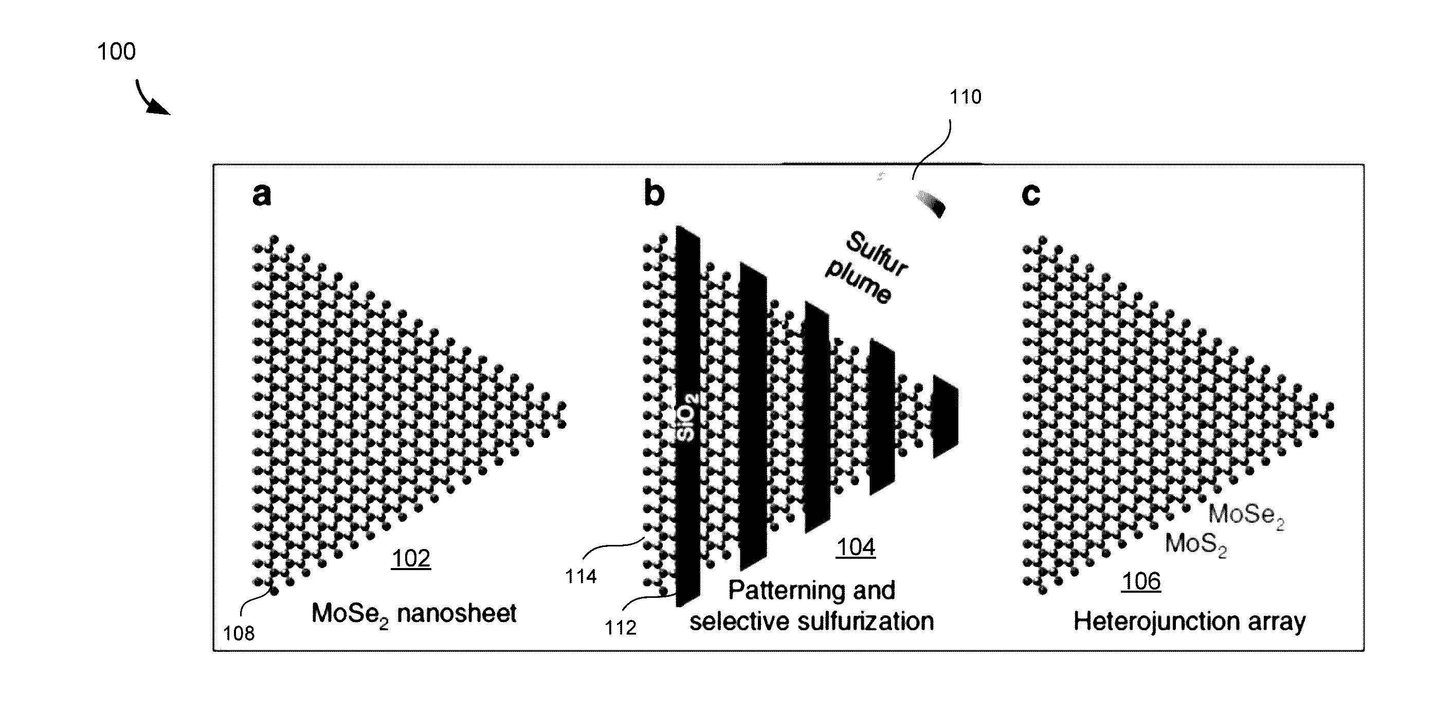
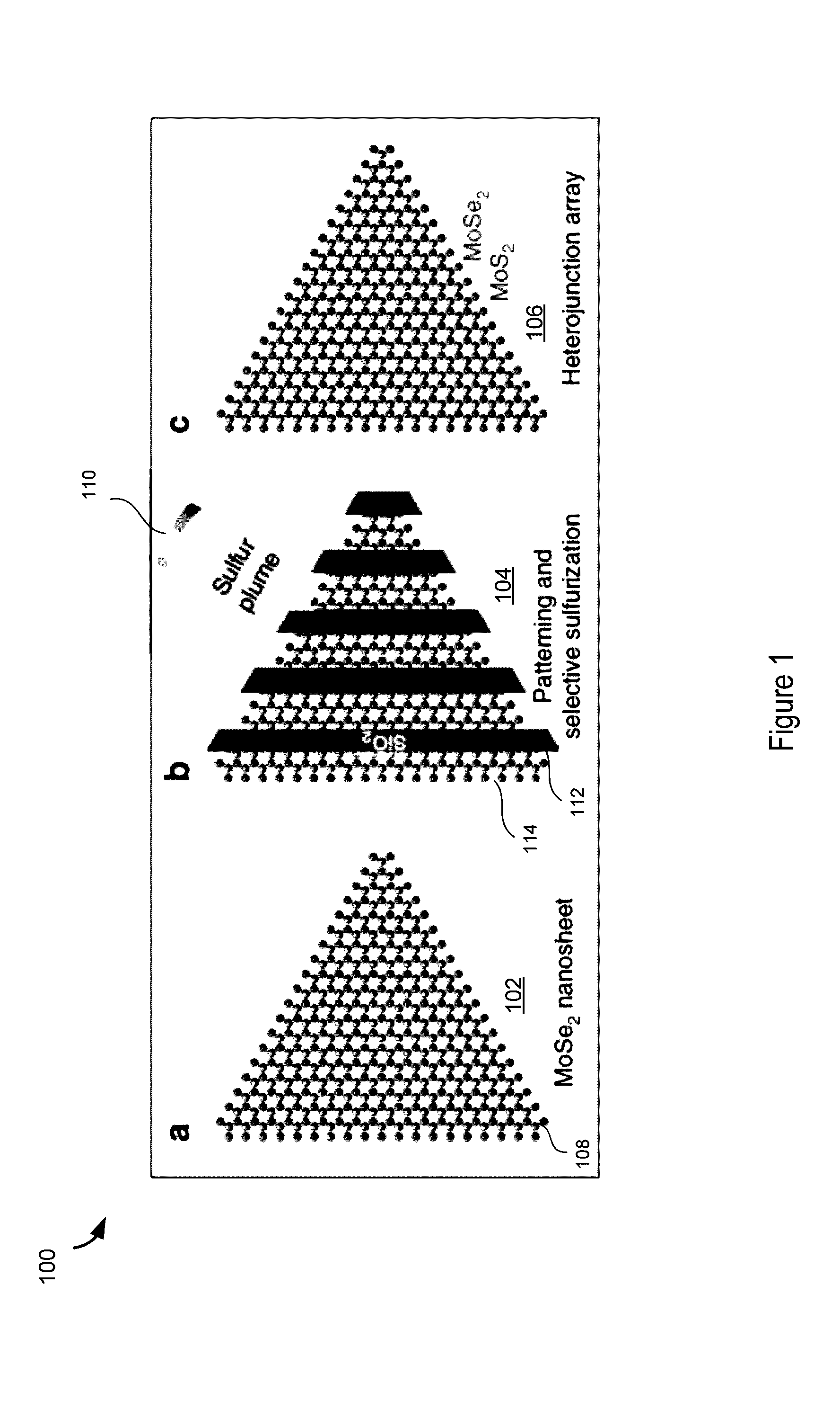
- A method involving lithographic patterning and pulsed laser deposition to convert specific regions of 2D materials from one composition to another, allowing for the precise formation of lateral heterojunctions, including p-n, n-n, and p-p junctions, within a single nanostructure layer, using techniques like electron beam lithography and high-kinetic energy pulsed laser vaporization.

Materials Characterization Techniques for Electride-2D Interfaces
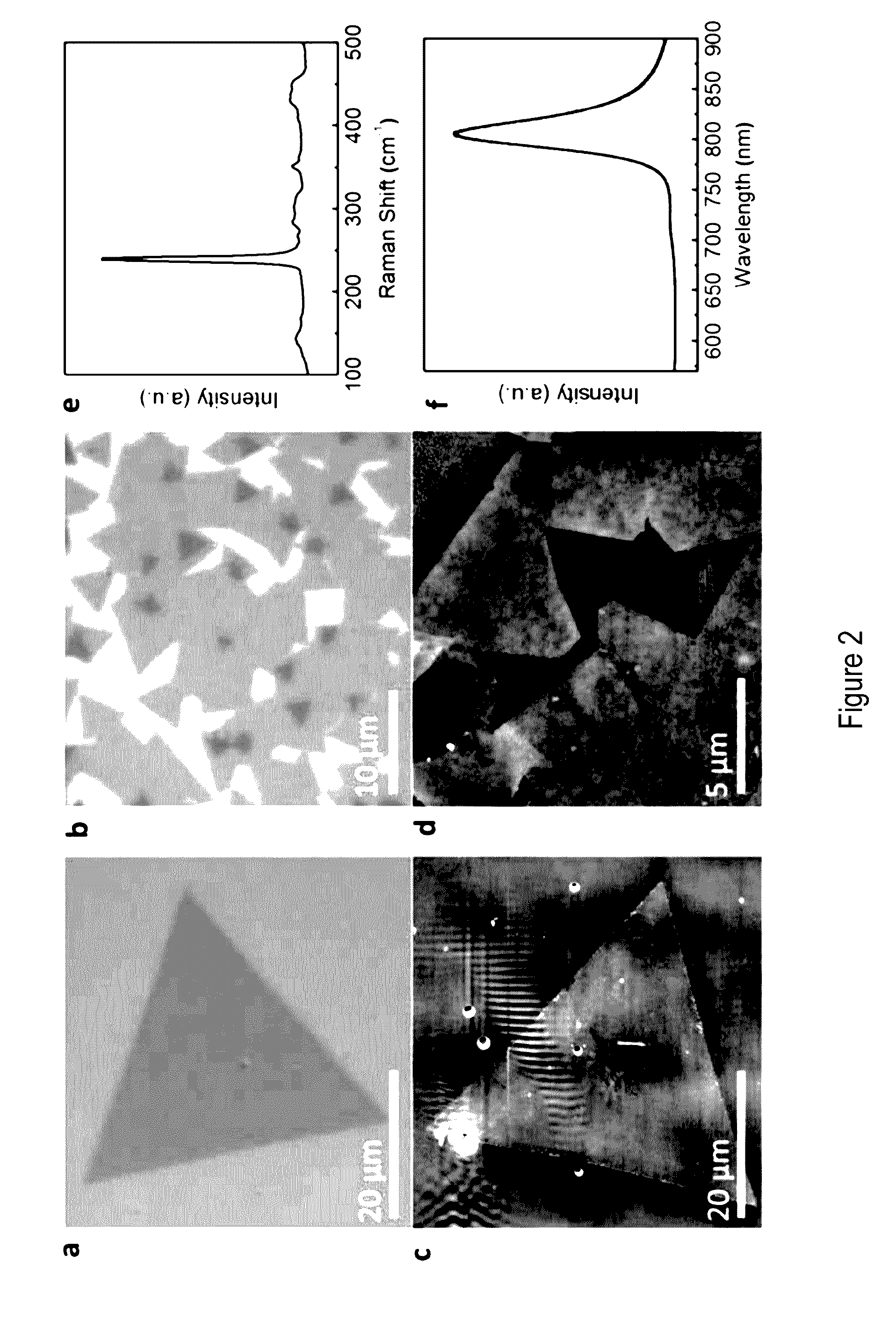
Characterizing the interfaces between electrides and 2D materials requires sophisticated analytical techniques to understand their structural, electronic, and chemical properties. X-ray diffraction (XRD) and high-resolution transmission electron microscopy (HRTEM) serve as primary tools for structural analysis, revealing atomic arrangements and crystallographic orientations at these unique interfaces. HRTEM particularly excels at visualizing the atomic-scale interactions between electrides and 2D materials, providing critical insights into interface quality and potential defects.
Scanning tunneling microscopy (STM) and atomic force microscopy (AFM) offer complementary surface-sensitive characterization capabilities. STM maps the electronic states at the interface with sub-nanometer resolution, while AFM provides topographical information and mechanical property measurements. These techniques are essential for understanding the morphology and electronic structure of electride-2D material heterostructures.
Spectroscopic methods including X-ray photoelectron spectroscopy (XPS) and ultraviolet photoelectron spectroscopy (UPS) enable detailed analysis of electronic states and chemical bonding at interfaces. XPS reveals elemental composition and chemical states, while UPS provides valuable information about work function and valence band structure. Angle-resolved photoemission spectroscopy (ARPES) further elucidates band structure modifications resulting from interface formation.
Raman spectroscopy has emerged as a powerful non-destructive technique for probing vibrational modes in 2D materials and their interfaces with electrides. Changes in peak positions, intensities, and widths can indicate strain, doping effects, and interfacial interactions. When combined with tip-enhanced Raman spectroscopy (TERS), nanoscale spatial resolution becomes possible, enabling mapping of local variations across interfaces.
Advanced synchrotron-based techniques, including X-ray absorption spectroscopy (XAS) and X-ray magnetic circular dichroism (XMCD), provide element-specific electronic and magnetic information. These techniques are particularly valuable for understanding charge transfer processes and magnetic coupling at electride-2D material interfaces, which are critical for spintronic applications.
In-situ and operando characterization methods represent the frontier of interface analysis, allowing real-time observation of interface formation and evolution under various environmental conditions. Techniques such as environmental TEM and ambient-pressure XPS enable studies of interface dynamics during growth processes or under operational conditions, providing insights that are inaccessible through ex-situ measurements.
Quantum Properties and Electronic Applications of Electride-2D Systems
The quantum properties of electride-2D material interfaces represent a frontier in condensed matter physics with significant implications for next-generation electronic applications. These hybrid systems exhibit unique quantum behaviors stemming from the interaction between the quasi-free electrons in electrides and the confined electronic states in 2D materials.
Quantum confinement effects at these interfaces lead to distinctive electronic band structures, where the electron density distribution can be precisely controlled through external stimuli. The resulting quantum wells at electride-2D interfaces demonstrate tunable quantum states, with electron mobility values exceeding 10,000 cm²/Vs in optimal configurations, surpassing many conventional semiconductor interfaces.
Particularly noteworthy is the emergence of topological states in certain electride-2D material combinations. For instance, Ca₂N electride interfaces with graphene have demonstrated signatures of quantum spin Hall effect at temperatures approaching 100K, significantly higher than most topological insulator materials. These topological properties arise from the strong spin-orbit coupling induced at the interface, creating protected edge states with potential applications in quantum computing.
The quantum coherence properties of these interfaces also merit attention, with coherence times reaching microsecond ranges in low-temperature environments. This characteristic makes electride-2D systems promising candidates for quantum information processing applications, particularly in quantum bit (qubit) architectures that require long coherence times.
From an electronic applications perspective, electride-2D interfaces offer several advantages over conventional semiconductor technologies. Field-effect transistors utilizing these interfaces have demonstrated on/off ratios exceeding 10⁶ with subthreshold swings approaching the theoretical limit of 60 mV/decade at room temperature. The low contact resistance at these interfaces (typically <100 Ω·μm) enables efficient charge injection, addressing a critical challenge in 2D material electronics.
Optoelectronic applications benefit from the unique light-matter interactions at electride-2D interfaces. Photodetectors based on these systems have shown broadband responsivity from ultraviolet to infrared wavelengths, with response times in the nanosecond range and specific detectivity values exceeding 10¹² Jones, competitive with commercial photodetection technologies.
The quantum capacitance effects observed at these interfaces also enable novel energy storage applications, with capacitance densities reaching 15-20 μF/cm², significantly higher than conventional electrical double-layer capacitors. This property, combined with the high electrical conductivity of electrides, positions these hybrid systems as promising candidates for next-generation supercapacitors.
Unlock deeper insights with PatSnap Eureka Quick Research — get a full tech report to explore trends and direct your research. Try now!
Generate Your Research Report Instantly with AI Agent
Supercharge your innovation with PatSnap Eureka AI Agent Platform!