EUV Masks And Pellicles: Materials Challenges And Readiness
AUG 22, 20259 MIN READ
Generate Your Research Report Instantly with AI Agent
Patsnap Eureka helps you evaluate technical feasibility & market potential.
EUV Lithography Background and Objectives
Extreme Ultraviolet (EUV) lithography represents a revolutionary advancement in semiconductor manufacturing technology, enabling the continuation of Moore's Law by facilitating the production of increasingly smaller transistors. The development of EUV lithography began in the 1980s, but significant technological breakthroughs only emerged in the early 2000s. This technology operates at a wavelength of 13.5nm, substantially shorter than the 193nm used in traditional deep ultraviolet (DUV) lithography, allowing for the creation of semiconductor features below 7nm.
The evolution of EUV technology has been marked by persistent challenges in source power, mask infrastructure, and resist performance. Initially, EUV systems struggled with insufficient light source power, limiting throughput and commercial viability. However, advancements in CO2 laser-produced plasma technology have gradually increased source power from less than 10W to over 250W in recent years, making high-volume manufacturing feasible.
A critical component of EUV lithography is the mask technology, which has evolved from traditional chrome-on-glass designs to complex multilayer reflective structures. These masks must maintain exceptional flatness and defect control at the atomic level to ensure pattern fidelity. The development trajectory shows a continuous refinement in mask blank manufacturing, defect inspection capabilities, and repair technologies.
The primary objective of current EUV mask and pellicle research is to address several interconnected challenges. First, to develop mask materials and structures that minimize pattern distortions caused by the non-telecentricity of EUV optical systems. Second, to create pellicle materials that can withstand the intense EUV radiation while maintaining transparency and thermal stability. Third, to establish inspection and repair methodologies capable of detecting and addressing defects at increasingly smaller dimensions.
Looking forward, the industry aims to extend EUV lithography to enable high-volume manufacturing at the 3nm node and beyond. This requires significant improvements in mask absorber materials to enhance contrast and reduce shadowing effects, as well as the development of more durable pellicle materials that can survive the higher source powers needed for future production requirements.
The technological roadmap also includes the potential transition to high-NA (numerical aperture) EUV systems, which would further reduce the printable feature size but introduce additional challenges for mask and pellicle technologies, including more stringent flatness requirements and increased thermal load management needs.
Market Demand Analysis for EUV Mask Technology
The global semiconductor industry has witnessed a significant shift towards Extreme Ultraviolet (EUV) lithography technology in recent years, driving substantial market demand for advanced EUV mask technologies. According to market research, the global EUV mask market was valued at approximately $1.2 billion in 2022 and is projected to grow at a compound annual growth rate (CAGR) of 17.5% through 2028, potentially reaching $3.5 billion by that time.
This robust market growth is primarily fueled by the semiconductor industry's relentless pursuit of Moore's Law, which necessitates increasingly smaller transistor sizes. The transition to 5nm, 3nm, and upcoming 2nm process nodes has made EUV lithography indispensable, consequently boosting demand for compatible mask technologies.
Leading semiconductor manufacturers, including TSMC, Samsung, and Intel, have announced significant capital expenditures for EUV lithography equipment, with combined investments exceeding $20 billion over the next five years. These investments directly translate to increased demand for EUV masks and pellicles, as each new fabrication line requires multiple sets of masks.
The market demand is further segmented by application areas. Logic chip manufacturing currently accounts for approximately 65% of EUV mask demand, followed by memory chip production at 25%, with the remaining 10% distributed across other specialized applications. This distribution reflects the technology adoption patterns across different semiconductor segments.
Geographically, East Asia dominates the market demand, with Taiwan, South Korea, and Japan collectively representing over 70% of global consumption. North America accounts for approximately 20%, while Europe represents about 8% of the market. This regional distribution closely mirrors the global semiconductor manufacturing landscape.
A critical market driver is the increasing complexity of chip designs, which requires more mask layers per device. Advanced processors now require over 80 mask layers, with approximately 15-20 being EUV masks. This multiplication effect significantly amplifies market demand beyond the simple growth in wafer starts.
The market also faces supply constraints, particularly regarding pellicle materials that can withstand EUV radiation while maintaining transparency. This has created premium pricing opportunities for suppliers who can deliver reliable solutions, with some specialized EUV masks commanding prices up to five times higher than traditional optical masks.
Looking forward, industry analysts predict continued strong demand growth as EUV technology extends to more applications and manufacturing nodes. The emergence of high-NA EUV systems will create additional market segments for specialized masks designed to leverage the enhanced resolution capabilities of these next-generation tools.
EUV Masks and Pellicles: Current Challenges
Extreme Ultraviolet (EUV) lithography represents a revolutionary advancement in semiconductor manufacturing, enabling the production of increasingly smaller and more complex integrated circuits. However, the implementation of EUV technology faces significant challenges, particularly in the development of masks and pellicles that can withstand the extreme conditions of EUV exposure.
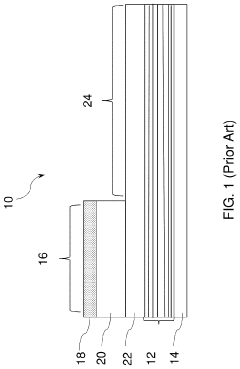
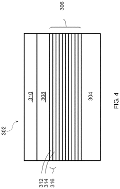
EUV masks differ fundamentally from traditional optical masks, requiring complex multilayer structures that reflect rather than transmit light. These masks consist of 40-50 alternating layers of molybdenum and silicon, each only a few nanometers thick, designed to reflect EUV light at the 13.5nm wavelength. The precision required for these multilayer structures presents extraordinary manufacturing challenges, with defects as small as 50nm potentially causing critical pattern failures.
The absorber materials used in EUV masks present another significant challenge. Traditional chrome-based absorbers are inadequate for EUV wavelengths, necessitating the development of new materials like tantalum-based compounds. These materials must simultaneously provide high absorption of EUV radiation, minimal impact on reflection phases, and compatibility with existing repair and inspection technologies.
Mask pattern distortion represents a persistent issue in EUV lithography. The non-telecentricity of EUV optical systems leads to shadowing effects and pattern shifts that become increasingly problematic as feature sizes shrink below 10nm. These distortions require complex computational corrections and innovative mask designs to ensure accurate pattern transfer.
Pellicles, thin membranes that protect masks from contamination, face even more extreme challenges in the EUV environment. The intense energy of EUV radiation (91.6 eV photons) rapidly degrades traditional pellicle materials. Current pellicle candidates, including silicon-based membranes, graphene, and metal-doped carbon nanomaterials, struggle to maintain the required 90% transmission rate while withstanding temperatures exceeding 1000°C during exposure.
The inspection and repair of EUV masks present unique difficulties due to their reflective nature and multilayer structure. Conventional inspection tools cannot detect all relevant defects, particularly those buried within the multilayer stack. Additionally, repairing defects without damaging the underlying reflective layers requires novel approaches and specialized equipment.
Manufacturing yield and cost effectiveness remain significant barriers to widespread EUV adoption. The complexity of EUV mask fabrication results in extended production times and lower yields compared to conventional photomasks. Current EUV mask costs exceed $300,000 per mask, with pellicles adding substantial additional expense, creating economic challenges for all but the most advanced semiconductor nodes.
Contamination control presents another critical challenge, as even nanometer-scale particles can cause fatal defects. The absence of robust pellicle solutions exacerbates this issue, requiring extraordinary clean room conditions and innovative approaches to particle detection and removal throughout the mask lifecycle.
Current Material Solutions for EUV Masks
01 EUV mask materials and structures
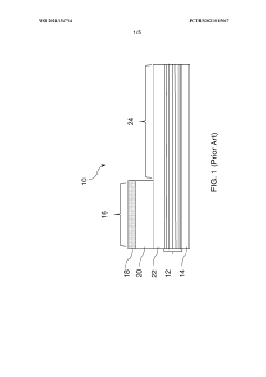
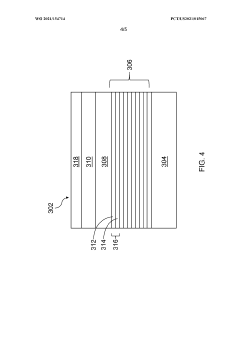
EUV masks require specialized materials to effectively reflect extreme ultraviolet radiation. These masks typically consist of multilayer reflective coatings, often made of alternating layers of molybdenum and silicon, deposited on a substrate. The structure may include absorber patterns made of materials like tantalum-based compounds that create the circuit pattern by absorbing EUV radiation. The precise thickness and composition of these layers are critical for achieving the desired optical properties and pattern transfer accuracy in EUV lithography.- EUV mask substrate materials: EUV mask substrates require specific materials with low thermal expansion coefficients and high flatness to maintain pattern accuracy during exposure. These substrates typically consist of ultra-low expansion glass or glass-ceramics that can withstand the intense energy of EUV radiation while maintaining dimensional stability. The substrate materials must also be capable of being polished to extreme smoothness to minimize defects that could affect pattern transfer.
- Reflective multilayer coatings for EUV masks: EUV masks utilize reflective multilayer coatings, typically consisting of alternating layers of molybdenum and silicon, to achieve high reflectivity at the 13.5 nm EUV wavelength. These multilayer stacks must be precisely engineered to maximize reflectivity while maintaining pattern fidelity. The thickness uniformity and interface quality between layers are critical factors affecting the performance of EUV masks in lithography systems.
- Pellicle membrane materials for EUV lithography: Pellicle membranes for EUV lithography must be extremely thin while maintaining high transmissivity at the 13.5 nm wavelength. These membranes are typically made from materials such as silicon, polysilicon, carbon-based films (including graphene), or metal-doped thin films. The pellicle material must withstand the high-energy EUV radiation without degradation while protecting the mask from contamination particles that could cause pattern defects.
- Absorber materials for EUV mask patterns: Absorber materials used in EUV masks must provide high absorption contrast at the 13.5 nm wavelength. Common absorber materials include tantalum-based compounds (such as TaBN or TaBO), chromium-based materials, and other high-atomic-number metals that effectively block EUV radiation. The absorber layer thickness and profile are optimized to minimize shadowing effects while maintaining pattern resolution and contrast during the lithography process.
- Inspection and defect mitigation for EUV masks and pellicles: Specialized techniques and materials are employed for inspection and defect mitigation in EUV masks and pellicles. These include actinic inspection tools that use EUV wavelengths to detect defects, as well as repair materials and methods to address identified issues. Advanced materials for defect compensation and pellicle handling frameworks are developed to maintain the integrity of these delicate components throughout the manufacturing process, ensuring high yield and performance in EUV lithography.
02 Pellicle materials for EUV lithography
Pellicles for EUV lithography require extremely thin membranes that can withstand intense EUV radiation while maintaining high transmittance. Materials such as silicon nitride, carbon-based films (including graphene and carbon nanotubes), and polysilicon are commonly used. These pellicle materials must balance several critical properties: thermal stability to withstand the heat generated by EUV absorption, mechanical strength despite being only a few nanometers thick, and sufficient transparency to EUV wavelengths around 13.5nm.Expand Specific Solutions03 Defect inspection and repair technologies
Advanced inspection and repair technologies are essential for EUV mask and pellicle manufacturing. These include electron beam inspection systems, actinic inspection tools that use EUV light for defect detection, and various repair methodologies. The inspection systems must be capable of detecting nanometer-scale defects that could impact pattern transfer. Repair technologies may involve focused ion beam systems, nanomachining techniques, or chemical processes to remove or add material at defect sites without damaging the surrounding mask or pellicle structure.Expand Specific Solutions04 Protective coatings and contamination control
Protective coatings and contamination control measures are crucial for extending the lifetime of EUV masks and pellicles. Various thin film coatings can be applied to protect the reflective multilayers from oxidation and carbon contamination. These may include ruthenium capping layers or other oxidation-resistant materials. Additionally, specialized cleaning processes and handling protocols are implemented to prevent particle contamination. Environmental control systems within EUV scanners maintain ultra-clean conditions to minimize contamination during exposure processes.Expand Specific Solutions05 Novel materials and manufacturing processes
Research into novel materials and manufacturing processes aims to overcome current limitations in EUV mask and pellicle technology. This includes exploration of alternative reflective multilayer compositions, such as ruthenium-silicon or zirconium-based materials, that may offer improved thermal stability or reflectivity. For pellicles, emerging approaches include atomic layer deposition techniques for creating ultra-uniform thin films, self-healing materials that can recover from radiation damage, and composite structures that combine different materials to achieve optimal optical and mechanical properties.Expand Specific Solutions
Key Industry Players in EUV Mask Ecosystem
The EUV mask and pellicle technology landscape is currently in a transitional phase, moving from early adoption to broader implementation as the semiconductor industry advances to smaller nodes. The market is experiencing rapid growth, projected to expand significantly as EUV lithography becomes essential for advanced chip manufacturing. Technologically, industry leaders like ASML, Taiwan Semiconductor Manufacturing Co., and Samsung Electronics have achieved production-ready EUV mask solutions, while companies such as Shin-Etsu Chemical, AGC, and Mitsui Chemicals are addressing materials challenges in pellicle development. Research institutions including IMEC and Korea Electronics Technology Institute collaborate with industry players to overcome persistent technical hurdles in thermal stability, transmission efficiency, and contamination control that currently limit broader EUV implementation.
Taiwan Semiconductor Manufacturing Co., Ltd.
Technical Solution: TSMC has developed proprietary EUV mask and pellicle solutions focused on manufacturing viability at scale. Their approach includes specialized multi-layer absorber stacks optimized for both high-volume manufacturing and advanced node requirements. TSMC's mask technology employs tantalum-based absorbers with precisely engineered thickness (approximately 55-70nm) to balance optical performance and pattern fidelity. For pellicles, TSMC has invested in carbon-based nanomaterials, particularly graphene and carbon nanotube composites, achieving transmission rates of approximately 90% while maintaining thermal stability at high EUV powers. Their mask inspection and repair protocols incorporate AI-driven defect detection systems that can identify critical defects as small as 10nm. TSMC has also pioneered specialized cleaning processes using hydrogen-based chemistries that effectively remove contaminants without damaging the delicate mask structures[2][5].
Strengths: Extensive practical implementation experience in high-volume manufacturing environments; integrated approach connecting mask technology directly to chip production yields; advanced defect management systems. Weaknesses: Solutions optimized for their specific manufacturing processes may have limited applicability to other fabrication environments; heavy reliance on external equipment suppliers for key technologies.
ASML Netherlands BV
Technical Solution: ASML has pioneered EUV lithography systems and developed comprehensive solutions for EUV masks and pellicles challenges. Their approach includes the development of advanced EUV pellicle technology based on polysilicon membranes with thickness of approximately 50nm, designed to withstand high-power EUV radiation (>250W) while maintaining transmission rates above 88%. ASML's pellicle framework utilizes specialized metal alloys that minimize thermal expansion and distortion during exposure. Their mask technology incorporates multi-layer reflective coatings with alternating molybdenum and silicon layers, precisely engineered to maximize EUV reflection at the 13.5nm wavelength. ASML has also developed specialized handling systems that minimize contamination risks during mask transfers and storage, addressing one of the critical challenges in EUV implementation[1][3].
Strengths: Industry-leading expertise in complete EUV ecosystem; vertical integration allowing synchronized development of exposure tools, masks, and pellicles; extensive R&D resources. Weaknesses: High dependency on complex supply chains for specialized materials; pellicle technology still faces durability challenges at higher EUV power levels required for future nodes.
Critical Patents and Innovations in EUV Pellicles
Extreme ultraviolet mask blank hard mask materials
PatentWO2021154714A1
Innovation
- The use of specific hard mask materials such as CrO, CrON, TaNi, TaRu, and TaCu, in combination with an antimony-containing absorber layer, is proposed to enhance etch selectivity, with the hard mask layer having an etch rate that is selectively higher or lower than the absorber layer to achieve desired etch ratios.
Extreme ultraviolet mask absorber materials
PatentActiveUS11640109B2
Innovation
- The use of a multilayer stack with a capping layer and an absorber layer comprising a compound of antimony and nitrogen, which is thinner than conventional absorber layers, to enhance reflectivity and reduce 3D mask effects by forming an EUV mask blank with a substrate and reflective layer pairs, allowing for precise control of absorber layer thickness and composition.
Supply Chain Resilience for EUV Materials
The global EUV lithography ecosystem faces significant supply chain vulnerabilities due to the highly specialized nature of materials required for mask and pellicle production. Current supply chains for critical EUV materials are characterized by geographic concentration, with Japan and the United States dominating the production of high-purity mask blanks, while European companies lead in pellicle membrane development. This concentration creates inherent risks in the event of geopolitical tensions, natural disasters, or public health emergencies.
Material sourcing represents a particular challenge for the EUV supply chain. The specialized glass-ceramic substrates used in EUV masks require rare earth elements and ultra-pure raw materials that often originate from politically sensitive regions. Similarly, the carbon-based nanomaterials used in pellicle production depend on specialized manufacturing capabilities available in only a handful of facilities worldwide.
The COVID-19 pandemic exposed critical weaknesses in the EUV materials supply chain, with production delays and logistics disruptions affecting the entire semiconductor manufacturing ecosystem. These disruptions highlighted the need for redundancy in supplier networks and geographic diversification of manufacturing capabilities to ensure continuity during global crises.
Industry leaders have begun implementing several strategies to enhance supply chain resilience. These include developing secondary supplier relationships, establishing strategic material reserves, and investing in alternative material research that could reduce dependence on scarce resources. Companies like ASML and its partners are also exploring vertical integration opportunities to gain greater control over critical material inputs.
Regulatory frameworks are evolving to address these vulnerabilities. The CHIPS Act in the United States and similar initiatives in Europe and Asia aim to strengthen domestic semiconductor ecosystems, including the materials supply chains that support EUV lithography. These policies include funding for research into alternative materials and manufacturing processes that could diversify supply options.
Long-term resilience will require collaborative industry approaches. Consortia such as SEMI's EUV Mask Infrastructure partnership are working to establish industry standards and shared facilities that can reduce single points of failure in the supply chain. Additionally, increased transparency in material sourcing and processing is becoming essential for identifying and mitigating potential disruptions before they impact production capabilities.
Environmental Impact of EUV Mask Production
The production of EUV masks involves complex manufacturing processes that generate significant environmental impacts across multiple dimensions. The high-precision nature of these components requires substantial energy consumption, particularly during the multi-layer deposition processes and pattern etching operations. Manufacturing facilities typically operate 24/7 climate-controlled cleanrooms that demand continuous power supply, contributing to considerable carbon footprints unless powered by renewable energy sources.
Water usage represents another critical environmental concern, with each mask requiring ultra-pure water for cleaning processes. A single manufacturing facility may consume millions of gallons annually, with the subsequent wastewater containing various chemicals and metal residues that require specialized treatment before discharge.
Chemical utilization in EUV mask production presents particular environmental challenges. The process employs numerous hazardous substances including strong acids, solvents, and specialized etching compounds. Many of these chemicals have high global warming potentials or ozone depletion properties. The industry has begun implementing closed-loop systems to recover and recycle these materials, though complete elimination of environmental discharge remains technically challenging.
Raw material extraction for EUV mask substrates and coatings creates upstream environmental impacts. The ultra-pure quartz and specialized metals required often involve energy-intensive mining and refining operations in various global locations, contributing to habitat disruption and potential water contamination at extraction sites.
Waste management presents ongoing challenges, as defective masks and production byproducts may contain combinations of hazardous materials requiring specialized disposal protocols. The industry has developed recycling techniques for recovering valuable materials from end-of-life masks, though these processes themselves consume additional energy and resources.
Recent industry initiatives have focused on developing more environmentally sustainable approaches to EUV mask production. These include implementing energy recovery systems, transitioning to less harmful chemical alternatives, and designing more efficient manufacturing processes that reduce resource requirements. Several leading manufacturers have established environmental targets for reducing their carbon footprints and hazardous waste generation by 30-50% over the next decade.
Regulatory frameworks governing EUV mask production vary significantly by region, with the European Union typically imposing the strictest environmental standards through directives like RoHS and REACH. Manufacturers increasingly adopt global standards exceeding local requirements to ensure consistent environmental performance across their international operations.
Unlock deeper insights with Patsnap Eureka Quick Research — get a full tech report to explore trends and direct your research. Try now!
Generate Your Research Report Instantly with AI Agent
Supercharge your innovation with Patsnap Eureka AI Agent Platform!