EUV Photoresists For High-NA Lithography: Materials, Stochastics, And Process Windows
AUG 22, 20259 MIN READ
Generate Your Research Report Instantly with AI Agent
Patsnap Eureka helps you evaluate technical feasibility & market potential.
EUV Photoresist Evolution and High-NA Lithography Goals
Extreme Ultraviolet (EUV) lithography has emerged as the cornerstone technology for advanced semiconductor manufacturing, enabling the continuation of Moore's Law beyond the limitations of traditional optical lithography. The evolution of EUV photoresists represents a critical technological trajectory that has unfolded over the past two decades, transitioning from experimental formulations to production-ready materials capable of supporting sub-10nm feature sizes.
Initially, EUV photoresist development focused on adapting 193nm immersion lithography materials, primarily based on chemically amplified resist (CAR) platforms. These early attempts revealed fundamental limitations in sensitivity, resolution, and line edge roughness—the classic "RLS trade-off" that continues to challenge material scientists. The progression from these early materials to current generation EUV photoresists has been marked by significant innovations in polymer design, photoacid generator chemistry, and quencher optimization.
The introduction of High Numerical Aperture (High-NA) EUV lithography, with NA values increasing from 0.33 to 0.55, represents the next inflection point in semiconductor manufacturing. This technological advancement aims to enable production of 3nm technology nodes and beyond, but simultaneously introduces unprecedented demands on photoresist performance. The primary goals for High-NA EUV photoresists include achieving sub-8nm half-pitch resolution while maintaining acceptable sensitivity (typically <30 mJ/cm²) and controlling stochastic failures to economically viable levels.
Material innovation for High-NA EUV photoresists is targeting several specific performance metrics: enhanced absorption efficiency to improve sensitivity, reduced blur length to enhance resolution, and novel molecular architectures to minimize stochastic variations. The industry has established ambitious targets including line edge roughness below 1.5nm (3σ), exposure latitude exceeding 10%, and defect densities below 0.01/cm².
The technological roadmap for EUV photoresists is increasingly focused on non-traditional approaches, including metal-oxide resists, molecular resists, and hybrid materials that can overcome the fundamental limitations of polymer-based systems. These novel materials aim to address the stochastic effects that become dominant at sub-10nm feature sizes, where individual photon absorption events and molecular-scale inhomogeneities significantly impact pattern fidelity.
As the semiconductor industry prepares for High-NA EUV implementation in high-volume manufacturing by 2025-2026, photoresist development has become a critical path technology. The ultimate goal is to create materials that can support multiple generations of device scaling while maintaining the economic viability of semiconductor manufacturing through acceptable process windows and defect rates.
Semiconductor Industry Demand for Advanced Lithography Solutions
The semiconductor industry's relentless pursuit of Moore's Law has driven demand for increasingly advanced lithography solutions. As transistor dimensions continue to shrink below 5nm, traditional lithography techniques have reached their physical limits, necessitating the adoption of Extreme Ultraviolet (EUV) lithography. The industry's transition to High Numerical Aperture (High-NA) EUV lithography represents the next critical evolution in semiconductor manufacturing technology.
Market analysis indicates that the global semiconductor industry, valued at approximately $573 billion in 2022, is projected to reach $1 trillion by 2030, with advanced nodes requiring EUV technology representing the highest growth segment. Leading semiconductor manufacturers including TSMC, Samsung, and Intel have collectively invested over $20 billion in EUV infrastructure, underscoring the strategic importance of this technology.
The demand for High-NA EUV lithography is primarily driven by the need to produce more powerful, energy-efficient chips for applications in artificial intelligence, high-performance computing, and mobile technologies. These applications require transistor densities exceeding 100 million transistors per square millimeter, achievable only through advanced lithography techniques.
Particularly significant is the growing demand from AI chip manufacturers, where computational requirements are doubling every 3-4 months, far outpacing Moore's Law. This acceleration has created urgent market pressure for lithography solutions capable of supporting the next generation of AI hardware.
The automotive and IoT sectors are emerging as secondary demand drivers, with requirements for specialized chips manufactured at advanced nodes. The automotive semiconductor market alone is expected to grow at a CAGR of 12.3% through 2028, with advanced driver-assistance systems and autonomous driving features requiring increasingly sophisticated processors.
Geopolitical factors have further intensified demand for domestic advanced lithography capabilities, with major economies investing in semiconductor sovereignty initiatives. The CHIPS Act in the United States, the European Chips Act, and similar programs in Asia collectively represent over $50 billion in government investment targeting advanced manufacturing capabilities.
Industry surveys indicate that 87% of semiconductor manufacturers consider advanced lithography solutions, particularly High-NA EUV technology, as critical to their competitive strategy. The development of suitable photoresists for High-NA EUV lithography has been identified as one of the top three technical challenges facing the industry, alongside power consumption and yield management.
High-NA EUV Photoresist Challenges and Technical Barriers
The advancement of extreme ultraviolet (EUV) lithography into the high numerical aperture (High-NA) regime presents unprecedented challenges for photoresist materials. As the industry transitions from 0.33 NA to 0.55 NA systems, photoresists must simultaneously meet more stringent requirements across multiple performance dimensions, creating a complex multi-variable optimization problem.
The fundamental challenge stems from the physics of High-NA EUV exposure. With shorter effective wavelengths and steeper angles of incidence, photons interact differently with resist materials, requiring significant reformulation of resist chemistry. The absorption characteristics that worked well for conventional EUV must be reconsidered for High-NA systems to maintain optimal exposure latitude.
Resolution capabilities present another critical barrier. High-NA EUV aims to enable sub-8nm features, but current photoresist materials struggle with line edge roughness (LER) and pattern collapse at these dimensions. The stochastic effects—random variations in photon absorption and chemical reactions—become increasingly dominant at smaller scales, creating statistical variations that can lead to catastrophic defects.
Sensitivity requirements create a particularly difficult trade-off. High-NA systems demand photoresists that can achieve adequate exposure with minimal dose to maximize throughput. However, lowering the dose exacerbates stochastic effects, while increasing it reduces productivity and raises concerns about pattern blur from secondary electron generation.
Chemical amplification mechanisms, which have been the backbone of photoresist technology, face limitations in the High-NA regime. The diffusion length of photoacid generators must be precisely controlled to prevent pattern blurring while maintaining sufficient sensitivity. This requires novel molecular architectures and inhibitor systems that can function reliably at atomic scales.
Process integration presents additional barriers. High-NA photoresists must be compatible with increasingly complex multilayer stacks and maintain performance across varying pattern densities. The process window—the range of exposure and focus conditions that produce acceptable patterns—narrows significantly for High-NA applications, requiring unprecedented precision in both materials and equipment.
Material uniformity at the molecular level becomes critical as feature sizes approach the dimensions of the resist molecules themselves. Conventional polymer-based resists face fundamental limitations in achieving the required homogeneity, driving research toward alternative approaches such as metal-oxide resists and molecular glasses.
The metrology challenge cannot be overlooked. Evaluating resist performance at High-NA dimensions requires advanced characterization techniques that can accurately measure sub-nanometer variations in pattern fidelity. This creates a feedback loop challenge where materials development is constrained by the ability to precisely measure performance.
Current High-NA EUV Photoresist Material Solutions
01 EUV photoresist composition optimization
Specialized photoresist compositions are developed specifically for EUV lithography to improve process windows and reduce stochastic effects. These compositions include specific polymers, photoacid generators, and additives that enhance sensitivity to EUV radiation while maintaining resolution and line edge roughness control. The formulations are designed to address the unique challenges of EUV lithography, including lower photon flux and higher energy absorption compared to traditional lithography methods.- EUV photoresist composition and formulation: Specialized photoresist compositions designed specifically for EUV lithography that address challenges of sensitivity, resolution, and line edge roughness. These formulations often include novel polymers, photoacid generators, quenchers, and additives that work together to improve process windows and reduce stochastic effects in EUV patterning. The chemical design of these materials is critical for achieving the balance between sensitivity and resolution required for advanced node manufacturing.
- Stochastic effects mitigation in EUV lithography: Methods and materials to reduce stochastic failures in EUV lithography, which occur due to photon shot noise and chemical inhomogeneity. These approaches include optimizing resist chemistry, exposure conditions, and post-exposure processing to minimize random variations in pattern formation. Techniques focus on controlling molecular distribution, improving photon absorption efficiency, and enhancing chemical amplification mechanisms to reduce statistical variations in the patterning process.
- Process window optimization for EUV lithography: Techniques for expanding the process window in EUV lithography by optimizing exposure parameters, development conditions, and post-processing steps. These methods aim to increase the tolerance for variations in focus, dose, and other process parameters while maintaining pattern fidelity. Approaches include dose modulation, focus control strategies, and advanced development techniques that collectively enhance the manufacturability of EUV lithographic processes.
- Metrology and characterization for EUV process control: Advanced measurement and inspection techniques specifically designed to characterize EUV photoresist performance, process windows, and stochastic variations. These methods include specialized imaging, scatterometry, and analytical techniques that provide insights into resist behavior at the nanoscale. The metrology approaches enable quantification of line edge roughness, critical dimension uniformity, and stochastic failures, which are essential for process optimization and control in EUV lithography.
- Multi-layer and underlayer strategies for EUV patterning: Implementation of multi-layer resist systems and specialized underlayers to improve EUV lithographic performance. These approaches use combinations of materials with different properties to enhance pattern transfer, reduce reflection, and improve adhesion. The layer stack design helps to optimize absorption of EUV radiation, control acid diffusion, and improve pattern fidelity, thereby expanding process windows and reducing stochastic failures in high-resolution patterning applications.
02 Stochastic effects mitigation techniques
Various techniques are employed to mitigate stochastic effects in EUV lithography, which arise from shot noise and material inhomogeneities. These include specialized exposure strategies, post-exposure treatments, and material modifications that reduce random variations in the photoresist response. By controlling these stochastic effects, the process window can be widened, allowing for more consistent pattern formation and improved yield in semiconductor manufacturing.Expand Specific Solutions03 Process window enhancement methods
Methods to enhance the process window for EUV photoresists include multi-layer resist approaches, optimized post-exposure bake conditions, and development process modifications. These techniques aim to increase the latitude for exposure dose and focus variations while maintaining pattern fidelity. Advanced process control systems are implemented to monitor and adjust process parameters in real-time, compensating for variations and extending the usable process window.Expand Specific Solutions04 Advanced metrology and characterization
Advanced metrology and characterization techniques are essential for understanding and optimizing EUV photoresist performance. These include specialized imaging methods, scatterometry, and analytical techniques that can detect nanoscale variations in resist patterns. Real-time monitoring systems help identify stochastic failures and process window limitations, enabling feedback for process optimization and material development to improve overall lithographic performance.Expand Specific Solutions05 Novel EUV resist platforms
Novel resist platforms are being developed specifically for EUV lithography, including metal-based resists, molecular resists, and hybrid materials. These new platforms aim to overcome the limitations of traditional chemically amplified resists by offering higher sensitivity, improved resolution, and reduced stochastic variations. The novel materials are designed with molecular architectures that enhance EUV absorption efficiency and provide more uniform chemical reactions during exposure, resulting in wider process windows.Expand Specific Solutions
Leading Manufacturers and Research Institutions in EUV Materials
The EUV photoresists for high-NA lithography market is in an early growth phase, characterized by intensive R&D activities and strategic positioning by key players. The market is projected to expand significantly as semiconductor manufacturers transition to advanced nodes, with an estimated value reaching several billion dollars by 2028. Technologically, the field remains challenging with companies at varying maturity levels. Industry leaders like ASML, Tokyo Electron, and TSMC are driving innovation in equipment integration, while materials specialists including DuPont, JSR, and Irresistible Materials focus on developing novel resist formulations. Samsung and Intel are actively investing in process optimization, while academic institutions like Chinese Academy of Sciences contribute fundamental research. The ecosystem reflects a competitive landscape where collaboration between equipment manufacturers, material suppliers, and chip producers is essential for overcoming stochastic effects and process window challenges.
Intel Corp.
Technical Solution: Intel has developed a comprehensive High-NA EUV resist strategy as part of their "angstrom-era" process technology roadmap. Their approach combines materials innovation with advanced computational lithography techniques to address the fundamental stochastic challenges of High-NA EUV. Intel's technology includes proprietary resist formulations with enhanced sensitivity (requiring <30mJ/cm² exposure dose) while maintaining resolution capabilities for sub-8nm features. Their materials science team has pioneered hybrid resist systems that incorporate both chemical amplification and metal-oxide components, leveraging the advantages of both approaches. Intel's process window optimization includes specialized post-exposure bake protocols that control acid diffusion with nanometer precision, significantly reducing line edge roughness. Their integrated approach includes customized development processes that minimize pattern collapse in high-aspect-ratio features, a critical concern for High-NA lithography. Intel collaborates extensively with material suppliers to co-develop resist formulations specifically optimized for their process requirements, creating tailored solutions for different device layers with varying resolution and line edge roughness requirements[9][10].
Strengths: Vertical integration allowing coordinated development of materials and processes; substantial research resources; ability to customize solutions for specific device requirements. Weaknesses: Historically less experienced in EUV implementation compared to TSMC; internal development may limit broader ecosystem benefits; significant pressure to accelerate development to maintain competitive position.
Taiwan Semiconductor Manufacturing Co., Ltd.
Technical Solution: TSMC has developed a comprehensive High-NA EUV photoresist integration strategy as part of their sub-2nm node development. Their approach focuses on process window optimization through co-optimization of resist materials with exposure and pattern development parameters. TSMC employs advanced computational lithography techniques including source-mask optimization (SMO) and inverse lithography technology (ILT) that compensate for the limitations of current resist materials. Their process integrates specialized underlayers and topcoats that enhance the performance of commercially available High-NA resists, achieving line edge roughness below 2nm for critical dimensions. TSMC has pioneered multi-patterning techniques specifically adapted for High-NA EUV that relax the resolution requirements for resist materials while maintaining overall pattern fidelity. Their approach includes advanced metrology systems that provide real-time feedback for process control, enabling tight distribution of critical dimensions despite stochastic variations inherent in EUV exposure processes[7][8].
Strengths: Unmatched process integration expertise; ability to optimize entire lithography system rather than just resist materials; practical manufacturing implementation experience. Weaknesses: Dependent on external suppliers for resist materials; solutions often involve process complexity rather than fundamental material improvements; competitive pressures limit sharing of technological breakthroughs.
Critical Innovations in Stochastic Effects Mitigation
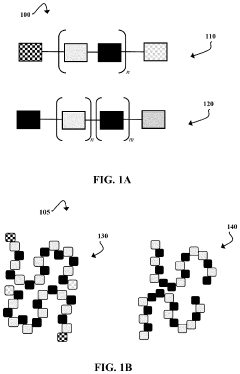
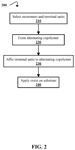
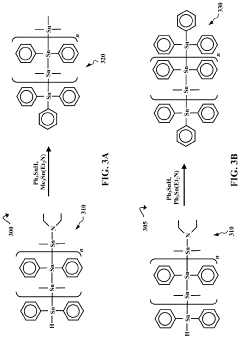
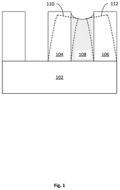
Alternating copolymer chain scission photoresists
PatentActiveUS11906901B2
Innovation
- Development of alternating copolymers with EUV-absorbing elements, such as Sn, Te, or Bi, that undergo chain scission upon EUV radiation exposure, eliminating the need for minority components like chemical amplifiers, and incorporating unreactive terminal units to control polymer chain lengths and prevent inter-chain reactions.
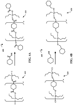
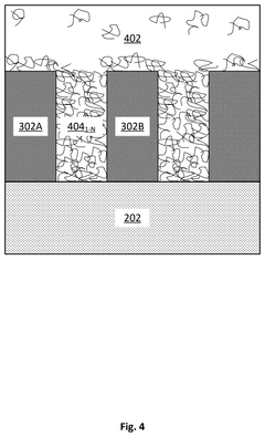
Semiconductor pattern structure preservation
PatentPendingUS20250201559A1
Innovation
- A method involving the deposition of a metal oxide resist layer, formation of pattern structures, application of a treatment composition with polymeric compounds, and tethering these compounds to the pattern structures to prevent collapse or distortion.
Environmental and Safety Considerations for EUV Materials
The environmental and safety considerations for EUV photoresist materials have become increasingly important as High-NA EUV lithography advances toward commercial implementation. These advanced materials present unique challenges that extend beyond traditional photoresist concerns, requiring comprehensive assessment and mitigation strategies throughout their lifecycle.
EUV photoresists contain metal-based compounds, particularly tin and antimony, which pose potential environmental contamination risks if not properly managed. These metals can persist in ecosystems and may bioaccumulate in living organisms. Recent studies indicate that tin-based photoresists demonstrate higher environmental persistence compared to traditional organic photoresists, necessitating specialized waste treatment protocols in semiconductor manufacturing facilities.
Worker safety represents another critical dimension, as EUV photoresist processing involves exposure to potentially harmful chemicals and nanoparticles. The fine particulate matter generated during development and etching processes may present respiratory hazards. Additionally, the photochemical reactions triggered by EUV radiation can produce reactive species with unknown toxicological profiles. Comprehensive industrial hygiene protocols, including enhanced ventilation systems and personal protective equipment, are essential for minimizing occupational exposure.
Regulatory frameworks governing these materials continue to evolve globally. The European Union's REACH regulations have placed increasing scrutiny on metal-organic compounds used in semiconductor manufacturing, while similar regulatory developments are emerging in North America and Asia. Manufacturers must navigate this complex regulatory landscape while maintaining innovation momentum in High-NA EUV technology development.
Sustainable design principles are increasingly being incorporated into new EUV photoresist formulations. Research efforts focus on developing materials with reduced environmental footprints, including biodegradable components and lower metal content. Several leading semiconductor materials suppliers have launched initiatives to develop "green photoresists" specifically designed for EUV applications, though these alternatives must still meet the stringent performance requirements of High-NA lithography.
Waste management strategies for EUV photoresist materials require specialized approaches. Conventional wastewater treatment methods may be insufficient for removing metal components, necessitating advanced filtration and chemical precipitation techniques. Closed-loop recycling systems that recover valuable metals from waste streams represent a promising direction, potentially transforming an environmental liability into a resource conservation opportunity.
Industry collaboration has emerged as a key factor in addressing these challenges. Consortia involving materials suppliers, equipment manufacturers, and semiconductor companies are developing standardized protocols for handling, disposal, and recycling of EUV photoresist materials. These collaborative efforts aim to establish best practices that balance technological advancement with environmental stewardship and worker protection.
Economic Impact Analysis of High-NA EUV Implementation
The implementation of High-NA EUV lithography represents a significant economic inflection point for the semiconductor industry, with far-reaching implications across the global technology supply chain. Initial capital expenditure for High-NA EUV equipment is projected to exceed $300 million per tool, approximately 1.5 times the cost of current EUV systems, creating substantial barriers to entry for all but the most capitalized semiconductor manufacturers.
When factoring in the specialized photoresist materials required for High-NA EUV processes, operational costs are expected to increase by 30-40% compared to current EUV nodes. However, economic modeling suggests that the enhanced resolution capabilities will enable a 25-30% reduction in cost-per-function at mature yields, potentially justifying these investments for high-volume manufacturing of advanced logic and memory devices.
The transition to High-NA EUV will likely accelerate industry consolidation, with only 3-5 global manufacturers expected to implement this technology at scale by 2026. This concentration may create significant regional economic disparities, as countries hosting these advanced facilities will gain disproportionate advantages in the high-value semiconductor supply chain.
Material supply economics present another critical dimension, as specialized High-NA EUV photoresists require rare elements and complex synthesis processes. Current market analysis indicates potential supply constraints that could impact implementation timelines, with photoresist costs projected to represent 7-9% of total process costs, up from 4-5% in current nodes.
Workforce economics must also be considered, as High-NA EUV implementation demands highly specialized engineering talent. Regions with established semiconductor education pipelines may experience significant economic advantages through talent concentration and associated innovation ecosystems.
The broader economic ripple effects extend to adjacent industries, with High-NA EUV enabling next-generation computing architectures that could generate $1-2 trillion in new market opportunities across artificial intelligence, quantum computing, and advanced telecommunications by 2030. However, these benefits must be weighed against the environmental economics of implementation, as High-NA EUV processes may increase energy consumption by 15-20% per wafer compared to current technologies.
Risk-adjusted ROI models suggest that despite the substantial upfront investments, early adopters of High-NA EUV technology could achieve breakeven within 3-4 years of implementation, assuming successful resolution of current photoresist challenges and achievement of target yield improvements.
Unlock deeper insights with Patsnap Eureka Quick Research — get a full tech report to explore trends and direct your research. Try now!
Generate Your Research Report Instantly with AI Agent
Supercharge your innovation with Patsnap Eureka AI Agent Platform!