Negative-Tone EUV Resists For High-Aspect-Ratio Etch Integration
AUG 22, 20259 MIN READ
Generate Your Research Report Instantly with AI Agent
Patsnap Eureka helps you evaluate technical feasibility & market potential.
EUV Lithography Background and Objectives
Extreme Ultraviolet (EUV) lithography represents a revolutionary advancement in semiconductor manufacturing technology, enabling the continuation of Moore's Law beyond the limitations of traditional optical lithography methods. The development of EUV lithography began in the 1980s, but significant technological breakthroughs only emerged in the early 2000s. This technology operates at a wavelength of 13.5 nm, substantially shorter than the 193 nm used in conventional deep ultraviolet (DUV) lithography, allowing for the patterning of significantly smaller features.
The evolution of EUV technology has been marked by several critical milestones, including the development of reliable EUV light sources, high-precision optics, and compatible photoresist materials. Initially, the primary challenges centered around generating sufficient power from EUV sources and creating effective reflective optics, as traditional refractive lenses absorb EUV radiation. By 2019, leading semiconductor manufacturers began implementing EUV lithography in high-volume manufacturing, signaling a new era in chip fabrication.
The current technological trajectory points toward further refinement of EUV processes, with particular emphasis on photoresist materials that can deliver both high resolution and high sensitivity while maintaining acceptable line edge roughness. Negative-tone EUV resists have emerged as a promising area of development due to their potential advantages in specific applications, particularly those requiring high-aspect-ratio features.
The primary objective of advancing negative-tone EUV resists for high-aspect-ratio etch integration is to enable the fabrication of increasingly complex three-dimensional structures necessary for next-generation semiconductor devices. These structures are essential for continued scaling in logic and memory applications, where vertical integration has become as important as lateral scaling for increasing transistor density.
Specifically, the technical goals include developing resist materials that can achieve sub-10 nm resolution with aspect ratios exceeding 5:1, while simultaneously providing sufficient etch resistance to withstand subsequent processing steps. Additionally, these materials must demonstrate compatibility with existing manufacturing workflows, minimal pattern collapse, and reduced line edge roughness to ensure device performance and yield.
The pursuit of these objectives aligns with the broader semiconductor industry roadmap, which anticipates continued device scaling through at least 2030. Success in this domain would enable the production of more powerful, energy-efficient integrated circuits for applications ranging from high-performance computing and artificial intelligence to mobile devices and Internet of Things (IoT) technologies, thereby sustaining the exponential growth in computing capabilities that has transformed modern society.
Market Demand for Negative-Tone EUV Resists
The semiconductor industry's continuous pursuit of Moore's Law has driven the development of advanced lithography techniques, with Extreme Ultraviolet (EUV) lithography emerging as the critical technology for sub-7nm nodes. Within this context, negative-tone EUV resists specifically designed for high-aspect-ratio (HAR) etch integration are experiencing rapidly growing market demand across multiple segments.
The global market for EUV lithography materials is projected to reach $1.2 billion by 2026, with negative-tone resists representing a significant growth segment. This demand is primarily driven by the semiconductor manufacturing industry's need to produce increasingly complex 3D structures and deep trenches with precise dimensions at advanced nodes.
Leading semiconductor manufacturers, including TSMC, Samsung, and Intel, have expressed strong interest in negative-tone EUV resists due to their superior etch resistance and pattern transfer capabilities. These companies are actively seeking solutions that can enable HAR features with aspect ratios exceeding 10:1 while maintaining critical dimension uniformity below 2nm.
Memory manufacturers represent another significant market segment, with DRAM and NAND flash producers requiring HAR structures for capacitor trenches and vertical channel formations. The market for negative-tone EUV resists in memory applications alone is expected to grow at 18% CAGR through 2025, outpacing the overall resist market growth of 12%.
Industry surveys indicate that 78% of semiconductor manufacturers consider improved HAR etch integration capabilities as "critical" or "very important" for their technology roadmaps beyond the 3nm node. This represents a substantial increase from 45% just three years ago, highlighting the accelerating demand trajectory.
From a geographical perspective, East Asia dominates the market demand, accounting for approximately 65% of global consumption, followed by North America at 22% and Europe at 13%. This distribution closely mirrors the regional concentration of advanced semiconductor manufacturing facilities.
The market is further characterized by specific performance requirements that drive demand for specialized negative-tone EUV resist formulations. Key parameters include etch selectivity exceeding 10:1 relative to underlying layers, line edge roughness below 2nm, and sensitivity improvements that enable throughput of at least 120 wafers per hour in high-volume manufacturing environments.
Foundry services for advanced nodes represent the fastest-growing segment, with annual growth rates exceeding 25% as more fabless semiconductor companies transition their designs to 5nm and below. This trend is expected to continue as artificial intelligence, high-performance computing, and advanced mobile applications drive demand for cutting-edge semiconductor devices that rely on HAR structures.
Technical Challenges in High-Aspect-Ratio Etch Integration
The integration of negative-tone EUV resists with high-aspect-ratio (HAR) etch processes presents significant technical challenges that must be addressed for successful implementation in advanced semiconductor manufacturing. The fundamental issue lies in the inherent trade-off between resolution, sensitivity, and line edge roughness (LER) - commonly known as the RLS triangle. As feature sizes continue to shrink below 10nm, maintaining pattern fidelity while achieving the necessary aspect ratios becomes increasingly difficult.
One of the primary challenges is pattern collapse during development. Negative-tone resists typically form cross-linked networks upon exposure, but the capillary forces during wet development can cause high-aspect-ratio features to collapse or deform. This becomes particularly problematic when aspect ratios exceed 5:1, which is increasingly common in advanced node requirements.
Etch selectivity presents another critical challenge. The negative-tone resist must maintain sufficient etch resistance to withstand aggressive plasma etching processes while transferring patterns into underlying hard mask or device layers. Current negative-tone EUV resist formulations often struggle to provide the necessary etch selectivity for HAR applications, particularly when compared to traditional positive-tone chemically amplified resists (CARs).
Resolution limitations also impact HAR integration. While EUV lithography theoretically enables feature sizes below 10nm, achieving clean, well-defined patterns with negative-tone resists at these dimensions remains challenging. The resolution is often limited by acid diffusion in chemically amplified systems or by insufficient cross-linking density in non-chemically amplified alternatives.
Material outgassing during EUV exposure represents another significant concern. The high-energy EUV photons (13.5nm wavelength) can cause resist components to volatilize, potentially contaminating the expensive EUV optics. Negative-tone resists must be carefully engineered to minimize outgassing while maintaining their patterning performance.
Line edge roughness and line width roughness (LER/LWR) become increasingly problematic at smaller dimensions. The stochastic effects inherent to EUV exposure are amplified in negative-tone systems, leading to potential variations in critical dimensions that can compromise device performance. This is particularly challenging for HAR structures where even small variations can significantly impact the final device characteristics.
Post-etch residue removal presents additional integration challenges. The cross-linked nature of negative-tone resists can make them difficult to remove completely after pattern transfer, potentially leading to defects or reliability issues in the final devices. Specialized stripping processes must be developed that effectively remove resist residues without damaging the underlying device structures.
Current Negative-Tone EUV Resist Solutions
01 Polymer-based negative-tone EUV resist compositions
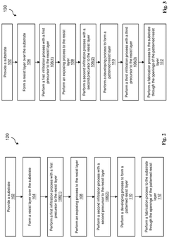
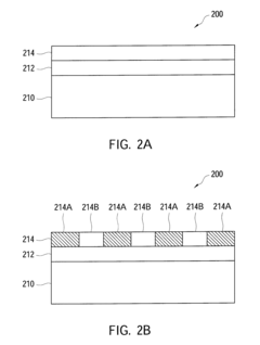
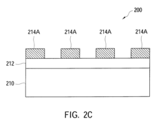
Polymer-based negative-tone EUV resist compositions are designed to achieve high-aspect-ratio patterns. These compositions typically include specific polymers with functional groups that undergo crosslinking upon exposure to EUV radiation. The crosslinking mechanism enhances pattern stability and resolution, allowing for the formation of high-aspect-ratio structures. These resists often incorporate acid generators and quenchers to control the crosslinking reaction and improve pattern fidelity.- Composition of negative-tone EUV resists for high aspect ratio: Specific chemical compositions can be formulated to create negative-tone EUV resists capable of achieving high aspect ratios. These compositions typically include photoacid generators, crosslinking agents, and polymers with specific functional groups that undergo crosslinking upon exposure to EUV radiation. The careful selection and balance of these components enable the formation of highly resolved patterns with steep sidewalls and high aspect ratios.
- Crosslinking mechanisms for negative-tone EUV resists: Various crosslinking mechanisms can be employed in negative-tone EUV resists to achieve high aspect ratios. These mechanisms include acid-catalyzed crosslinking, radical-initiated crosslinking, and hybrid approaches. The crosslinking reaction creates insoluble regions in exposed areas, while unexposed areas remain soluble in the developer, resulting in negative-tone patterns with high structural integrity and aspect ratios.
- Development processes for high aspect ratio structures: Specialized development processes are crucial for achieving high aspect ratio structures with negative-tone EUV resists. These processes may involve specific developer solutions, development temperatures, and techniques such as critical point drying to prevent pattern collapse. The development process must be carefully optimized to maintain the integrity of fine features while removing unexposed resist material, thereby enabling the formation of high aspect ratio structures.
- Post-exposure treatment techniques: Post-exposure treatment techniques can significantly enhance the aspect ratio capabilities of negative-tone EUV resists. These techniques include post-exposure baking to promote crosslinking reactions, flood exposure to increase crosslinking density, and various hardening treatments. Such treatments can improve the mechanical strength and etch resistance of the resist patterns, allowing for the creation of stable high aspect ratio structures.
- Integration with etching processes for pattern transfer: The integration of negative-tone EUV resists with subsequent etching processes is essential for transferring high aspect ratio patterns to underlying substrates. This integration requires careful consideration of the resist's etch resistance, selectivity, and compatibility with various etching chemistries. Advanced etching techniques, such as atomic layer etching and directional reactive ion etching, can be employed to maintain the high aspect ratio during pattern transfer.
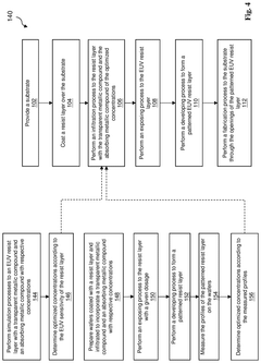
02 Metal-containing EUV resist materials for high-aspect-ratio patterning
Metal-containing materials in negative-tone EUV resists can significantly enhance sensitivity and pattern quality for high-aspect-ratio structures. These materials incorporate metal atoms or clusters that increase EUV absorption efficiency and improve resist performance. The metal components can include organometallic compounds, metal oxide nanoparticles, or metal salts that contribute to the crosslinking mechanism. This approach enables the formation of narrower, deeper features with improved line edge roughness and pattern collapse resistance.Expand Specific Solutions03 Development processes for high-aspect-ratio negative-tone EUV resists
Specialized development processes are crucial for achieving high-aspect-ratio features in negative-tone EUV resists. These processes include optimized developer solutions, development temperatures, and techniques such as supercritical fluid development or solvent vapor annealing. The development parameters significantly impact the final pattern quality, with careful control needed to prevent pattern collapse while maintaining high resolution. Advanced development techniques can enhance aspect ratios by improving the removal of unexposed resist while preserving crosslinked structures.Expand Specific Solutions04 Additives and modifiers for enhancing high-aspect-ratio performance
Various additives and modifiers can be incorporated into negative-tone EUV resist formulations to enhance high-aspect-ratio performance. These include dissolution inhibitors, adhesion promoters, plasticizers, and radical scavengers. Such additives help control the crosslinking reaction, improve adhesion to substrates, reduce internal stress in resist patterns, and enhance mechanical stability of high-aspect-ratio features. The careful selection and optimization of these components can significantly improve pattern quality and prevent defects like pattern collapse.Expand Specific Solutions05 Post-exposure treatment methods for high-aspect-ratio negative-tone EUV resists
Post-exposure treatment methods play a critical role in achieving high-aspect-ratio features in negative-tone EUV resists. These treatments include post-exposure baking (PEB), flood exposure, plasma treatments, and thermal annealing processes. Such treatments can enhance crosslinking density, improve pattern stability, and reduce line edge roughness. Advanced techniques like controlled atmosphere processing or sequential multi-step treatments can further optimize the mechanical properties of resist patterns, enabling higher aspect ratios without pattern collapse.Expand Specific Solutions
Key Industry Players in EUV Resist Development
The negative-tone EUV resist market for high-aspect-ratio etch integration is in a growth phase, driven by advanced semiconductor manufacturing demands. The market is expanding as EUV lithography adoption increases, with an estimated value exceeding $500 million. Technologically, the field is maturing but still evolving, with key players demonstrating varying levels of expertise. Industry leaders include JSR, Tokyo Ohka Kogyo, and Shin-Etsu Chemical developing advanced resist formulations, while semiconductor giants like TSMC, Samsung, and SK hynix drive application requirements. Equipment manufacturers ASML and Lam Research provide complementary technologies. Research institutions like MIT and University of Amsterdam collaborate with industry to overcome technical challenges in resist sensitivity, resolution, and line edge roughness for next-generation semiconductor devices.
Shin-Etsu Chemical Co., Ltd.
Technical Solution: Shin-Etsu has developed advanced negative-tone EUV resist materials based on their proprietary metal-oxide nanoparticle technology. Their approach incorporates hafnium and zirconium oxide nanoparticles into polymer matrices to enhance EUV sensitivity while maintaining high resolution. The company's latest formulations achieve aspect ratios exceeding 5:1 in sub-20nm features through careful engineering of the resist's crosslinking mechanism. Their metal-oxide hybrid resists demonstrate sensitivity below 20 mJ/cm² while maintaining line edge roughness (LER) under 3nm. Shin-Etsu has also implemented novel quencher compounds that control acid diffusion during post-exposure bake, enabling sharper pattern profiles and improved critical dimension uniformity. Their EUV resist platform incorporates specialized dissolution inhibitors that enhance contrast between exposed and unexposed regions, critical for high-aspect-ratio pattern transfer.
Strengths: Superior etch resistance due to metal-oxide incorporation, excellent pattern fidelity at high aspect ratios, and compatibility with existing semiconductor manufacturing processes. Weaknesses: Higher material costs compared to traditional resists, potential for metal contamination requiring additional cleaning steps, and more complex formulation requiring specialized handling.
FUJIFILM Corp.
Technical Solution: FUJIFILM has pioneered negative-tone EUV resist technology through their multi-trigger resist platform specifically designed for high-aspect-ratio applications. Their approach utilizes a hybrid system combining chemical amplification with non-chemically amplified mechanisms to achieve optimal sensitivity-resolution-roughness balance. FUJIFILM's latest formulations incorporate nano-phase separation technology where specialized block copolymers create self-organizing domains that enhance both EUV absorption and pattern transfer characteristics. Their resists achieve aspect ratios of 6:1 for 15nm features through precisely controlled crosslinking chemistry that minimizes pattern collapse. The company has developed proprietary PAG (photoacid generator) systems with reduced diffusion lengths, enabling sharper pattern profiles essential for high-aspect-ratio structures. FUJIFILM's negative-tone resists also incorporate specialized metal-organic compounds that significantly improve etch selectivity (>10:1 versus silicon) while maintaining compatibility with standard development processes.
Strengths: Exceptional pattern collapse resistance even at high aspect ratios, superior etch selectivity enabling deeper pattern transfer, and excellent compatibility with existing lithography equipment. Weaknesses: Requires precise process control parameters that may limit manufacturing flexibility, higher sensitivity to environmental contaminants, and more complex post-exposure processing requirements.
Critical Patents and Research in EUV Resist Chemistry
Extreme ultraviolet photolithography method with infiltration for enhanced sensitivity and etch resistance
PatentActiveUS12111576B2
Innovation
- Incorporating a metal-containing chemical into the photoresist through an infiltration process, such as atomic layer deposition or chemical vapor deposition, to enhance EUV sensitivity and etch resistance, allowing the photoresist to be more effective under EUV radiation and improve patterning accuracy.


Photoresist and patterning process
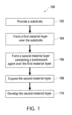
PatentInactiveUS20120003582A1
Innovation
- Incorporating a luminescent agent into the photoresist coating that absorbs short-wavelength EUV light and converts it into longer-wavelength UV-Vis light, which can be absorbed by PAGs to generate acid, thereby improving acid generation efficiency and reducing heat generation.
Material Science Advancements for EUV Resist Performance
Recent advancements in material science have significantly propelled the development of negative-tone EUV resists, particularly for high-aspect-ratio (HAR) etch integration applications. The molecular architecture of these resist materials has undergone substantial refinement, with researchers focusing on optimizing cross-linking mechanisms that enhance resolution while maintaining structural integrity during the etching process.
Polymer chemistry innovations have introduced novel monomeric units with improved sensitivity to EUV radiation, allowing for more efficient pattern formation at lower exposure doses. These developments have addressed previous limitations in negative-tone resists, where sensitivity often came at the expense of resolution or line edge roughness (LER).
Metal-organic frameworks (MOFs) have emerged as promising candidates for next-generation negative-tone EUV resists. Their highly ordered crystalline structures provide exceptional mechanical stability during high-aspect-ratio etching processes, while their tunable chemical properties allow for precise control over dissolution behavior in developer solutions.
Nanocomposite materials incorporating inorganic components have demonstrated enhanced etch resistance, a critical parameter for HAR applications. Silicon, hafnium, and zirconium-based nanoparticles strategically incorporated into organic matrices have shown up to 30% improvement in etch selectivity compared to conventional organic resists, enabling aspect ratios exceeding 10:1 in production environments.
Surface modification techniques have revolutionized the interface properties of negative-tone resists. Advanced grafting methodologies and self-assembled monolayers have improved adhesion to substrates while reducing pattern collapse in high-aspect-ratio features. These innovations have extended the practical limits of negative-tone resist performance in demanding semiconductor manufacturing processes.
Molecular weight distribution control has emerged as a crucial factor in optimizing resist performance. Narrow polydispersity indices achieved through controlled polymerization techniques have resulted in more uniform cross-linking density, directly translating to improved critical dimension uniformity across wafers.
Additives and sensitizers specifically designed for EUV wavelengths have enhanced quantum yield in photochemical reactions, addressing the fundamental challenge of photon shot noise in EUV lithography. These compounds effectively amplify the chemical changes induced by EUV photons, improving sensitivity without compromising resolution capabilities.
Environmental stability enhancements through novel stabilizing agents have extended the shelf life and process latitude of negative-tone resists. These advancements have made negative-tone EUV resists increasingly viable for high-volume manufacturing environments where consistency and reliability are paramount.
Environmental and Safety Considerations in Resist Development
The development of negative-tone EUV resists for high-aspect-ratio etch integration must carefully consider environmental and safety implications throughout the research, manufacturing, and disposal lifecycle. Current EUV resist formulations often contain metal-based compounds and complex organic molecules that pose significant environmental challenges and potential health hazards.
Chemical components in negative-tone EUV resists, particularly organometallic compounds containing elements like tin, antimony, or zirconium, require stringent handling protocols due to their potential toxicity. These materials can bioaccumulate in aquatic environments when improperly disposed of, leading to long-term ecological damage. Additionally, the solvents used in resist formulations often include volatile organic compounds (VOCs) that contribute to air pollution and may have adverse health effects on workers in manufacturing environments.
Regulatory frameworks governing resist development have become increasingly stringent worldwide. The European Union's REACH (Registration, Evaluation, Authorization and Restriction of Chemicals) regulations and similar initiatives in other regions mandate comprehensive safety assessments and documentation for chemical substances. Semiconductor manufacturers must navigate these complex regulatory landscapes while maintaining technological advancement in resist performance.
Waste management represents another critical environmental consideration. The semiconductor industry generates significant quantities of chemical waste during lithography processes, including partially used resists, developer solutions, and rinse water containing dissolved resist components. Advanced treatment technologies such as activated carbon filtration, chemical precipitation, and advanced oxidation processes are being implemented to minimize environmental impact from these waste streams.
Green chemistry principles are increasingly being applied to next-generation resist development. Research efforts focus on designing inherently safer materials through approaches such as reducing metal content, developing water-soluble alternatives, and creating biodegradable polymer platforms. These initiatives aim to maintain or enhance lithographic performance while reducing environmental footprint and occupational hazards.
Worker safety considerations in resist handling include exposure to potentially harmful chemicals through inhalation, skin contact, or accidental ingestion. Comprehensive industrial hygiene programs incorporating engineering controls (ventilation systems, enclosed processing equipment), administrative controls (standard operating procedures, training), and personal protective equipment are essential components of safe resist handling protocols.
Life cycle assessment (LCA) methodologies are being applied to evaluate the comprehensive environmental impact of resist materials from raw material extraction through manufacturing, use, and ultimate disposal. These assessments help identify opportunities for environmental optimization and guide the development of more sustainable resist technologies that balance performance requirements with environmental responsibility.
Unlock deeper insights with Patsnap Eureka Quick Research — get a full tech report to explore trends and direct your research. Try now!
Generate Your Research Report Instantly with AI Agent
Supercharge your innovation with Patsnap Eureka AI Agent Platform!