Resist Outgassing And Contamination Control For EUV Scanners
AUG 22, 202510 MIN READ
Generate Your Research Report Instantly with AI Agent
Patsnap Eureka helps you evaluate technical feasibility & market potential.
EUV Lithography Outgassing Background and Objectives
Extreme Ultraviolet (EUV) lithography represents a revolutionary advancement in semiconductor manufacturing, enabling the production of increasingly smaller and more complex integrated circuits. As the industry transitions to sub-7nm nodes, EUV technology has become indispensable for maintaining Moore's Law. However, the implementation of EUV lithography introduces unique challenges, particularly in the realm of resist outgassing and contamination control.
The evolution of EUV lithography technology spans over two decades, beginning with early research in the 1990s and culminating in the recent commercial deployment by leading semiconductor manufacturers. Throughout this development timeline, contamination issues have consistently presented significant obstacles to achieving optimal performance and reliability. The high-energy photons used in EUV processes (13.5nm wavelength) create unique interactions with photoresist materials, resulting in the release of volatile compounds that can contaminate critical optical components.
Historically, contamination control in lithography systems has evolved from relatively straightforward filtration methods to sophisticated multi-layered approaches combining chemical, physical, and thermal management strategies. The transition to EUV has dramatically elevated these challenges due to the vacuum environment required and the extreme sensitivity of reflective optics to even nanoscale contamination.
The primary technical objective in addressing EUV resist outgassing is to develop comprehensive solutions that minimize contamination while maintaining high throughput and yield. This involves understanding the fundamental mechanisms of outgassing, characterizing the chemical species involved, and implementing effective mitigation strategies throughout the lithography process.
Current industry goals include reducing outgassing rates by at least an order of magnitude compared to early EUV resist formulations, extending optical component lifetimes to economically viable levels, and establishing standardized testing methodologies to evaluate new resist materials. Additionally, there is significant focus on developing in-situ cleaning technologies that can restore contaminated optical surfaces without requiring system disassembly.
The technical trajectory suggests increasing integration of contamination control strategies directly into resist chemistry design, moving beyond mere mitigation toward fundamentally non-outgassing materials. Parallel development paths are exploring both chemical innovations in resist formulation and engineering solutions in scanner design, with the ultimate aim of creating a holistic ecosystem where contamination is managed at every stage from resist development through exposure and post-processing.
As EUV lithography continues to mature, the industry is establishing more refined metrics and specifications for outgassing control, driving collaborative efforts between equipment manufacturers, material suppliers, and semiconductor fabrication facilities to address this critical challenge.
Market Demand for Contamination-Free EUV Systems
The global semiconductor industry's shift toward Extreme Ultraviolet (EUV) lithography represents a pivotal technological advancement in chip manufacturing. Market research indicates that the EUV lithography equipment market is projected to grow at a CAGR of 21.5% from 2021 to 2026, reaching approximately $13.3 billion by 2026. This substantial growth is primarily driven by the increasing demand for contamination-free EUV systems that can produce smaller, more powerful, and energy-efficient semiconductor devices.
The market demand for contamination-free EUV systems stems from the critical need for higher resolution and precision in semiconductor manufacturing. As chip manufacturers continue to pursue Moore's Law by shrinking transistor sizes below 7nm, traditional DUV (Deep Ultraviolet) lithography has reached its physical limits. EUV lithography, operating at a 13.5nm wavelength, enables the production of smaller features but requires unprecedented levels of contamination control.
Leading semiconductor manufacturers like TSMC, Samsung, and Intel have collectively invested over $50 billion in EUV technology implementation. These investments reflect the urgent market need for contamination-free systems that can maintain production yields above 90% at advanced nodes. Industry reports indicate that even minor contamination in EUV systems can reduce yield rates by 15-20%, translating to millions in lost revenue per production line.
The financial implications of contamination control are substantial. A single high-end EUV scanner costs approximately $150 million, and contamination-related downtime can cost manufacturers up to $500,000 per day. This economic reality has created a robust market for advanced resist materials and contamination control solutions, estimated at $2.1 billion annually and growing at 18% year-over-year.
Consumer electronics companies are driving significant downstream demand for chips produced using contamination-free EUV processes. The smartphone market alone, valued at $448 billion, requires increasingly sophisticated chips for advanced features like AI processing and 5G connectivity. Similarly, the automotive industry's transition toward electric and autonomous vehicles has created new demand for high-performance, contamination-free semiconductor components.
Geographically, the market demand is concentrated in East Asia (particularly Taiwan, South Korea, and Japan), which accounts for approximately 65% of global demand for contamination-free EUV systems. North America and Europe represent secondary but growing markets at 20% and 15% respectively, driven by initiatives to strengthen domestic semiconductor manufacturing capabilities.
The market is further bolstered by governmental strategic initiatives worldwide. The US CHIPS Act, EU Chips Act, and similar programs in South Korea, Japan, and China collectively allocate over $200 billion toward semiconductor manufacturing advancement, with significant portions dedicated to next-generation lithography technologies including contamination-free EUV systems.
Current Challenges in Resist Outgassing Control
Despite significant advancements in EUV lithography technology, resist outgassing remains one of the most critical challenges facing the semiconductor industry. The extreme ultraviolet environment creates unique conditions where photoresist materials, when exposed to 13.5nm wavelength radiation, release volatile compounds that can contaminate critical optical surfaces. This contamination directly impacts scanner availability, throughput, and ultimately the economic viability of EUV technology implementation.
Current EUV resists face a fundamental dilemma: they must simultaneously provide high sensitivity, low line edge roughness, and minimal outgassing properties. These requirements often conflict with each other, as chemical modifications that enhance resolution performance frequently increase outgassing tendencies. Industry data indicates that typical EUV resists can release between 10-100 ng/cm² of volatile compounds during exposure, while scanner specifications demand levels below 5 ng/cm².
The vacuum environment of EUV scanners (operating at 10⁻⁷ to 10⁻⁹ Torr) exacerbates the contamination issue, as outgassed molecules have longer mean free paths and higher probability of reaching critical optical surfaces. Particularly concerning is carbon deposition on multilayer mirrors, which can reduce reflectivity by 1-2% per contamination layer, significantly degrading image quality and throughput over time.
Metrology challenges further complicate outgassing control efforts. Current measurement techniques like Residual Gas Analysis (RGA) and Quartz Crystal Microbalance (QCM) provide valuable data but lack the sensitivity and specificity needed for comprehensive outgassing characterization at the molecular level. This creates uncertainty in resist qualification processes and slows the development cycle for new materials.
Supply chain considerations present additional obstacles. The specialized nature of EUV resist formulations requires tight integration between resist suppliers, tool manufacturers, and end users. Proprietary formulation details are often closely guarded, limiting the semiconductor industry's ability to collaboratively address outgassing challenges through open innovation platforms.
Regulatory constraints are increasingly impacting resist development pathways. Environmental regulations limiting the use of certain fluorinated compounds and perfluorinated chemicals—historically valuable for their low outgassing properties—have forced material scientists to explore alternative chemistries with less established performance profiles.
The economic impact of these challenges is substantial. Unscheduled scanner downtime for cleaning contaminated optics can cost manufacturers millions of dollars per day in lost productivity. Additionally, the extended development cycles for outgassing-compliant resists delay the implementation of advanced nodes, affecting the entire semiconductor value chain and potentially slowing Moore's Law progression.
Existing Outgassing Mitigation Strategies
01 Contamination control in semiconductor manufacturing
Various methods and systems are employed in semiconductor manufacturing to control contamination. These include specialized cleaning processes, protective barriers, and monitoring systems to prevent particulate matter from affecting sensitive components. Advanced filtration systems and clean room technologies are implemented to maintain ultra-pure environments necessary for high-precision semiconductor fabrication, reducing defects and improving yield rates.- Contamination control in semiconductor manufacturing: Various methods and systems are employed in semiconductor manufacturing to control contamination. These include specialized cleaning processes, protective coatings, and environmental control systems that minimize particle generation. Advanced filtration systems and monitoring techniques are used to maintain clean room conditions and prevent contamination during wafer processing, which is critical for maintaining yield and device performance.
- Outgassing prevention in vacuum systems: Techniques to prevent outgassing in vacuum systems involve material selection, surface treatments, and specialized preparation methods. Materials with low outgassing properties are chosen for vacuum chamber components, and surfaces are treated to minimize gas release. Baking procedures and degassing techniques are implemented to remove adsorbed gases before operation. These measures are essential for maintaining high vacuum levels and preventing contamination in sensitive equipment.
- Contamination monitoring and detection systems: Advanced monitoring systems are used to detect and measure contamination in real-time. These include particle counters, gas analyzers, and optical inspection tools that can identify contaminants at microscopic levels. Automated monitoring systems provide continuous surveillance of critical environments, allowing for immediate corrective action when contamination is detected. These systems are crucial for maintaining quality control in sensitive manufacturing processes.
- Materials and coatings for contamination resistance: Specialized materials and coatings are developed to resist contamination and outgassing. These include low-outgassing polymers, anti-static coatings, and barrier films that prevent particle adhesion and gas release. Surface treatments that modify the chemical or physical properties of materials can significantly reduce contamination susceptibility. These materials are particularly important in aerospace, semiconductor, and optical applications where even minimal contamination can cause critical failures.
- Cleanroom design and contamination control protocols: Comprehensive cleanroom design and operational protocols are implemented to minimize contamination risks. These include airflow management systems, pressure differentials between zones, and strict personnel procedures. Specialized cleaning regimens, material transfer protocols, and equipment maintenance schedules are established to maintain cleanliness standards. These integrated approaches create controlled environments where sensitive processes can be performed with minimal contamination risk.
02 Outgassing prevention in vacuum systems
Techniques to prevent outgassing in vacuum systems involve specialized materials selection, surface treatments, and thermal processing. Materials with low outgassing properties are chosen for components used in vacuum environments. Pre-treatment processes such as baking, degassing, and surface conditioning help remove volatile compounds before assembly. These measures are critical in maintaining vacuum integrity and preventing contamination in sensitive equipment.Expand Specific Solutions03 Advanced materials for contamination resistance
Development of specialized materials with inherent contamination resistance properties has been a focus area for sensitive applications. These materials include modified polymers, composite structures, and surface-treated components that resist particle generation and chemical degradation. The materials are engineered to maintain stability under extreme conditions while minimizing the release of contaminants that could compromise system performance.Expand Specific Solutions04 Monitoring and detection systems for contamination control
Advanced monitoring systems are employed to detect and analyze contamination in real-time. These systems utilize various sensing technologies including optical detection, mass spectrometry, and particle counting to identify contaminants before they cause damage. Integrated software solutions provide data analysis and predictive maintenance capabilities, allowing for proactive contamination management and system protection in critical environments.Expand Specific Solutions05 Contamination control in lithography processes
Specialized techniques are implemented to control contamination in lithography processes, which are particularly sensitive to particulate matter and chemical impurities. These include environmental control systems, specialized resist formulations, and protective pellicles that shield photomasks from contaminants. Advanced cleaning protocols and handling procedures are also employed to maintain the integrity of optical components and substrates throughout the lithography process.Expand Specific Solutions
Leading Manufacturers and Research Institutions
The EUV scanner resist outgassing and contamination control market is in a growth phase, with increasing adoption of EUV lithography in advanced semiconductor manufacturing. The market is projected to expand significantly as chipmakers transition to sub-7nm nodes, creating a multi-billion dollar opportunity. Technologically, this field remains challenging due to the extreme sensitivity of EUV optics to molecular contamination. ASML dominates the EUV scanner market, working closely with Carl Zeiss SMT for optical systems. Key players like Taiwan Semiconductor Manufacturing Co. and Samsung Electronics drive requirements as end-users, while companies such as Lam Research, Tokyo Electron, and Gigaphoton contribute specialized solutions for contamination control. Research institutions including IMEC and Korea Electrotechnology Research Institute are advancing fundamental understanding of outgassing mechanisms and mitigation strategies, creating a competitive ecosystem balancing commercial interests with collaborative research.
Carl Zeiss SMT GmbH
Technical Solution: Zeiss SMT has pioneered specialized contamination control solutions for EUV optics, focusing on protecting their high-precision mirror systems. Their technology includes advanced capping layers for multilayer mirrors that resist contamination while maintaining reflectivity. Zeiss has developed proprietary surface treatments that reduce adsorption of outgassed species onto optical surfaces. Their contamination mitigation approach incorporates specialized gas curtain technology that creates protective barriers around critical optical components, preventing resist outgassing products from reaching sensitive surfaces. Additionally, Zeiss has implemented advanced thermal management systems that maintain precise temperature control to minimize thermally-induced outgassing effects. Their mirror protection systems include specialized coatings with self-cleaning properties that can withstand hydrogen radical cleaning processes without degradation[2][5].
Strengths: World-leading expertise in EUV optics protection; highly specialized surface treatments and coatings that maintain optical performance under contamination stress. Weaknesses: Solutions primarily focused on optical components rather than comprehensive scanner systems; requires integration with other vendors' technologies.
ASML Netherlands BV
Technical Solution: ASML has developed comprehensive contamination control solutions for their EUV lithography systems, including advanced vacuum and purge systems that minimize molecular contamination. Their NXE platform incorporates multi-layer contamination control strategies with specialized hydrogen radical cleaning (HRC) technology that removes carbon contamination from optical surfaces without damaging the underlying materials. ASML's systems feature integrated particle filters and specialized resist outgassing mitigation techniques including optimized pumping systems and sophisticated baffles that capture outgassed molecules before they can reach sensitive optical components. Their EUV scanners employ differential pumping zones that create pressure gradients to direct contaminants away from critical optical paths[1][3]. ASML has also developed specialized membrane technology that allows for effective separation between the wafer environment and the optical column.
Strengths: Market leader in EUV lithography with the most advanced contamination control systems integrated directly into scanner design; proprietary cleaning technologies for in-situ maintenance. Weaknesses: High system complexity increases maintenance requirements; solutions are primarily designed for their own equipment ecosystem rather than as standalone technologies.
Key Patents and Innovations in EUV Contamination Control
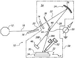
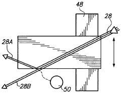
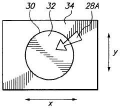
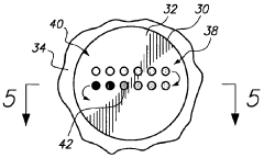
Resist exposure and contamination testing appparatus for EUV lithography
PatentWO2011037638A1
Innovation
- A resist exposure and contamination testing apparatus that uses a deflection mirror to block particulate matter and ions, a filter to remove visible light, and a multilayer concave mirror to focus EUV radiation onto a wafer, allowing for controlled exposure and detection of outgassing gases, while a witness sample assesses potential contamination effects on EUV stepper components.
Photolithography system
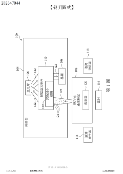
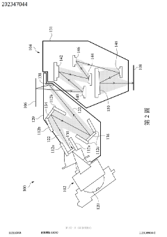
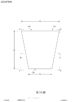
PatentPendingTW202347044A
Innovation
- Implementing contamination reduction structures with highly electronegative materials that adsorb and decompose contaminants before they accumulate on optical surfaces, maintaining the cleanliness of the scanner and preventing corrosion.

Environmental Impact and Sustainability Considerations
The environmental impact of EUV lithography systems, particularly regarding resist outgassing and contamination control, presents significant sustainability challenges for the semiconductor industry. Chemical compounds released during the photoresist exposure process can contaminate critical optical components, reducing system efficiency and increasing maintenance requirements. These outgassed materials often contain volatile organic compounds (VOCs) and other potentially hazardous substances that require specialized handling and disposal protocols.
The semiconductor manufacturing industry faces increasing regulatory pressure worldwide to minimize environmental footprints. EUV scanner operations involve multiple chemicals with varying environmental persistence and toxicity profiles. Resist materials and cleaning agents used in contamination control may contain perfluorinated compounds (PFCs) or other substances of emerging environmental concern, necessitating careful lifecycle management.
Energy consumption represents another critical environmental consideration. Contamination control systems, including advanced filtration, vacuum pumps, and thermal management components, contribute significantly to the already substantial energy demands of EUV lithography tools. Improving the energy efficiency of these systems while maintaining strict contamination control presents an important sustainability challenge.
Water usage in EUV processes also merits attention from a sustainability perspective. Ultrapure water systems for cleaning and contamination prevention consume substantial resources, while wastewater from these processes may contain trace amounts of photoresist compounds requiring specialized treatment before discharge.
The semiconductor industry has begun implementing circular economy principles to address these challenges. Strategies include developing photoresist materials with reduced environmental persistence, designing contamination control systems with lower energy requirements, and implementing closed-loop recycling for process chemicals and materials.
Leading equipment manufacturers are increasingly incorporating sustainability metrics into their technology roadmaps. This includes designing EUV scanners with improved material efficiency, reduced waste generation, and lower lifetime carbon footprints. The industry is also exploring alternative resist chemistries that maintain high resolution capabilities while reducing environmental impact through biodegradable components or reduced outgassing potential.
Collaborative industry initiatives, such as the Semiconductor Climate Consortium, are working to establish standardized sustainability benchmarks specifically addressing the unique environmental challenges of advanced lithography processes, including resist outgassing and contamination control in EUV systems.
Cleanroom Standards and Quality Assurance Protocols
In the context of EUV lithography systems, cleanroom standards and quality assurance protocols are critical for maintaining optimal performance and preventing contamination-related failures. The International Organization for Standardization (ISO) has established specific classifications for cleanrooms used in semiconductor manufacturing, with EUV scanner environments typically requiring ISO Class 3 (equivalent to Class 1 in the Federal Standard 209E) or cleaner to minimize particulate contamination.
Cleanroom protocols for EUV environments must address both particulate and molecular contamination. Particulate control involves HEPA and ULPA filtration systems that can capture particles as small as 0.1 microns with 99.9995% efficiency. These systems maintain laminar airflow patterns to prevent turbulence that could redistribute contaminants across sensitive optical components.
Molecular contamination control requires specialized gas filtration systems that can remove volatile organic compounds (VOCs) and other outgassing products. Chemical filters utilizing activated carbon and specialized sorbents are deployed to capture specific molecular contaminants known to affect EUV optics and resist performance.
Quality assurance for EUV cleanrooms incorporates continuous monitoring systems that track particle counts, temperature, humidity, and pressure differentials in real-time. Advanced monitoring techniques include residual gas analysis (RGA) to detect molecular contaminants at parts-per-billion levels. These systems typically feature automated alerts when parameters exceed predetermined thresholds.
Personnel protocols represent another critical aspect of contamination control. Strict gowning procedures using electrostatic discharge (ESD) safe materials minimize human-generated contamination. Multi-stage gowning rooms with air showers and tacky mats serve as contamination barriers between the external environment and the cleanroom proper.
Material qualification processes ensure that only compatible materials enter the EUV environment. This includes testing for outgassing characteristics using techniques such as thermal desorption spectroscopy (TDS) and gas chromatography-mass spectrometry (GC-MS). Materials must meet stringent outgassing specifications, typically below 1×10^-10 g/cm²/s for total mass loss.
Documentation and certification procedures form the backbone of quality assurance systems. Regular audits verify compliance with established protocols, while detailed contamination event investigations help refine preventive measures. Certification processes often involve third-party verification to ensure objectivity and compliance with industry standards.
Advanced cleanrooms for EUV applications increasingly incorporate automated material handling systems to minimize human intervention and associated contamination risks. These systems operate within strictly controlled environments and undergo regular validation to ensure continued performance within specification.
Unlock deeper insights with Patsnap Eureka Quick Research — get a full tech report to explore trends and direct your research. Try now!
Generate Your Research Report Instantly with AI Agent
Supercharge your innovation with Patsnap Eureka AI Agent Platform!